Light-emitting device and production method therefor

a light-emitting device and semiconductor technology, applied in the direction of semiconductor devices, basic electric elements, electrical equipment, etc., can solve the problems of further strain relaxation and insufficient elimination of strain, and achieve the effect of reducing the full width at half maximum of the emission spectrum, improving emission efficiency, and improving efficiency

Active Publication Date: 2017-09-26
TOYODA GOSEI CO LTD
View PDF5 Cites 0 Cited by
  • Summary
  • Abstract
  • Description
  • Claims
  • Application Information

AI Technical Summary

Benefits of technology

[0009]In view of the foregoing, an object of the present invention is to provide a Group III nitride semiconductor light-emitting device in which the strain applied to a light-emitting layer is reduced, thereby improving the emission efficiency.
[0013]The emission efficiency can be improved and the full width at half maximum of emission spectrum can be reduced by reducing the In composition ratio of the first well layer than the In composition ratios of the other well layers so that the emission wavelengths of the other well layers are equal to the emission wavelength of the first well layer. Equal emission wavelength may be a level that the emission wavelengths cannot be substantially distinguished from each other, for example, the absolute value of the emission wavelength difference is 2 nm or less.
[0014]Moreover, a difference between the In composition ratios of the other well layers and the In composition ratio of the first well layer is, preferably, more than 0% and less than 5.2%. Within this range, the emission efficiency can be further improved. The difference is, more preferably, 1% to 4.5%, and, further preferably, 2% to 3.5%.
[0015]The full width at half maximum of emission spectrum can be reduced by reducing the In composition ratio of the first well layer than the In composition ratios of the other well layers. For example, a light-emitting device having a half-value width of 20 nm or less can be achieved.
[0016]According to the present invention, the emission efficiency can be improved by reducing the strain applied to the first well layer without losing a light-emitting function of the first well layer.

Problems solved by technology

Although the strain can be reduced by generating pits as described in Japanese Patent Application Laid-Open (kokai) No. 2014-110396, the strain is not sufficiently eliminated, and further strain relaxation was required.

Method used


Image

  • Light-emitting device and production method therefor
  • Light-emitting device and production method therefor
  • Light-emitting device and production method therefor

Examples


embodiment 1

Structure of Light-Emitting Device

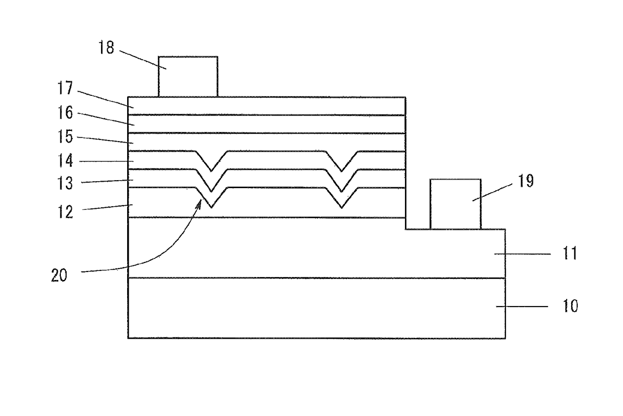
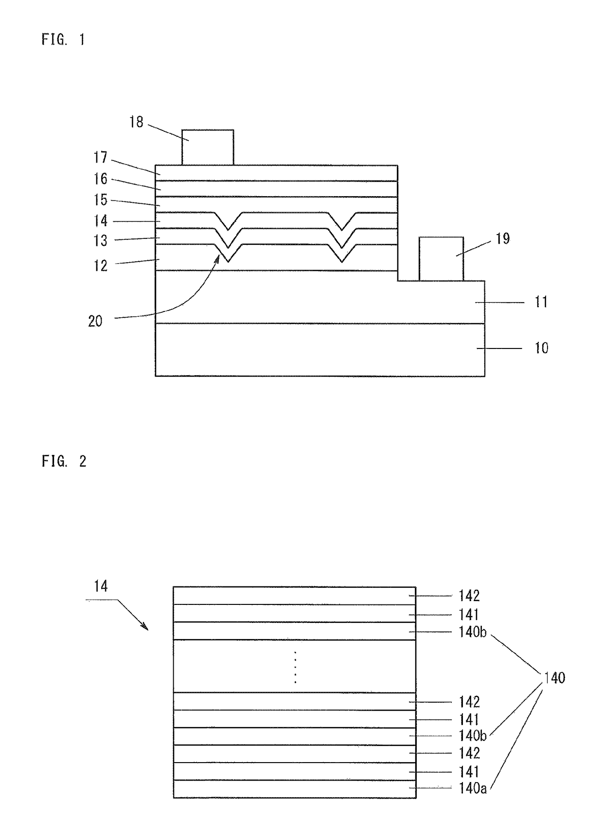
[0024]FIG. 1 is a sketch showing the structure of a Group III nitride semiconductor light-emitting device according to Embodiment 1. As shown in FIG. 1, the light-emitting device according to Embodiment 1 has a substrate 10. On the substrate 10, an n-type contact layer 11, an nESD layer 12, an n-type cladding layer 13, a light-emitting layer 14, a p-type cladding layer 15, and a p-type contact layer 16, each of them being made of Group III nitride semiconductor, are deposited via an AlN buffer layer (not illustrated). On the p-type contact layer 16, a transparent electrode 17 is provided, and on the transparent electrode 17, a p-electrode 18 is provided. A trench is formed on a part of a surface of the p-type contact layer 16, and the n-type contact layer 11 is exposed at the bottom surface of the trench. An n-electrode 19 is provided on the exposed n-type contact layer 11.

[0025]Next will be described the components of the light-emitting device acco...


PUM


Abstract

An emission efficiency of a light-emitting device is improved by reducing strains applied to a light-emitting layer. On a sapphire substrate, an n-type contact layer, an nESD layer, an n-type cladding layer, a light-emitting layer, a p-type cladding layer, and a p-type contact layer, are sequentially deposited. The light-emitting layer has a MQW structure in which a layer unit of a well layer, a capping layer, and a barrier layer sequentially deposited is repeatedly deposited. Of the well layers, the In composition ratio of only first well layer is reduced than the In composition ratios of other well layers, and the In composition ratios of the other well layers are equal to each other. The In composition ratio of the first well layer is designed so that the emission wavelength of the first well layer is equal to the emission wavelengths of other well layers.

Description

BACKGROUND OF THE INVENTION[0001]Field of the Invention[0002]The present invention relates to a Group III nitride semiconductor light-emitting device, more specifically, the one characterized by the structure of a light-emitting layer.[0003]Background Art[0004]In the Group III nitride semiconductor light-emitting device, a MQW structure in which a well layer and a barrier layer are repeatedly deposited is widely used as a light-emitting layer. The well layers are formed of InGaN and have the same In composition ratio.[0005]Japanese Patent No. 3433038 describes that the In composition ratios of a well layer closest to an n-type cladding layer and a well layer closest to a p-type cladding layer are reduced than the In composition ratio of a well layer at the center, thereby relaxing the strain applied from both the n-type cladding layer and the p-type cladding layer to a light-emitting layer.[0006]Japanese Patent Application Laid-Open (kokai) No. 2014-110396 describes that an nESD lay...

Claims


Application Information

Patent Timeline
Patent Type & Authority Patents(United States)
IPC IPC(8): H01L33/00H01L33/06H01L33/24H01L33/02H01L33/32
CPCH01L33/24H01L33/02H01L33/06H01L33/32
Inventor NAKAMURA, RYOBOYAMA, MISATO
Owner TOYODA GOSEI CO LTD
Why Eureka
Try Eureka