Liquid crystal panel

a liquid crystal panel and liquid crystal technology, applied in non-linear optics, instruments, optics, etc., to achieve the effect of finely expressing color and gradation, reducing wiring area, and reducing wiring area in the outside of the pixel region in the column direction

Active Publication Date: 2017-11-21
SAKAI DISPLAY PROD
View PDF7 Cites 0 Cited by
  • Summary
  • Abstract
  • Description
  • Claims
  • Application Information

AI Technical Summary

Benefits of technology

[0015]In consideration of the above-mentioned circumstances, it is an object of the present invention to provide a liquid crystal panel having a configuration that can reduce a wiring area with respect to an auxiliary capacitor in electrodes of each sub-pixel, and suppress wave rounding of a rectangular wave of a signal, thereby efficiently achieving a prevention of display unevenness, while coping with a request of slimmed border in a display apparatus using the liquid crystal panel.
[0023]According to the embodiment of the present invention, the auxiliary capacitor wirings connected to the auxiliary capacitors of the electrodes associating to the pixels in each row are classified into the groups in every plurality of rows, and the auxiliary capacitor wirings are connected with the branch wirings in the column direction for the groups at a plurality of locations. The branch wirings in the column direction are connected to the stem wirings which are wired in the row direction outside the pixel region for each group. The stem wirings arranged outside the pixel region are configured to be separated into a plurality of wirings, and are connected to the branch wirings of the same group for each separated unit wiring, such that, even on the same straight line, different unit wirings may be connected with the column wirings of the different groups. The different unit wirings on the same straight line may be used as the stem wirings of the groups, such that, it is possible to reduce a wiring area in the outside the pixel region in the column direction.
[0024]Further, the stem wirings may be wired outside the pixel region in the column direction. In this case, the stem wirings are connected to the branch wirings in the column direction through the auxiliary capacitor wirings for each group, and are further connected to other auxiliary capacitor wirings of the same group from the branch wirings. Also in this case, the stem wirings are configured to be separated into a plurality of wirings, and are connected to the respective separated unit wirings for the groups, such that, even on the same straight line, different unit wirings may be connected to the auxiliary capacitor wirings of the different groups. In this regards, the stem wirings in the row direction are not required, and the different unit wirings on the same straight line may be used as the stem wirings of the groups, such that it is possible to further reduce the wiring area outside the pixel region in the column direction.
[0025]According to the embodiment of the present invention, According to the present invention, the plurality of unit wirings are arranged in the column direction (or the row direction), but the number of the arranged unit wirings are smaller than the number of the groups. In the case where the branch wirings are connected to the stem wirings wired for the groups without being separated in the row direction, the number of the rows of the stem wirings is the number of the groups. However, by forming the stem wirings by the unit wirings arranged in the column direction (or the row direction) with the number smaller than the number of the groups, it is possible to reduce the wiring area in the outside the pixel region in the column direction.
[0028]According to the embodiment of the present invention, one pixel includes the plurality of sub-pixels for different colors or different light intensities, and the sub-pixels are arranged in a matrix state as a lattice shape within the same pixel. Each electrode and the auxiliary capacitor respectively associate to one sub-pixel. The auxiliary capacitor wirings connected to the auxiliary capacitors of each sub-pixel receive the signal through the stem wiring including the separated unit wirings. By the configuration in which one pixel corresponds to the plurality of sub-pixels for different colors or different light intensities, it is possible to finely express the color and gradation by the one pixel. Although the number of the auxiliary capacitors are increased, by the configuration of the stem wiring including the separated unit wirings, reducing the wiring area and maintaining a transfer rate of the signal to the auxiliary capacitor may be achieved.
[0029]According to the embodiment of the present invention, the wiring area in the outside the pixel region in the column direction can be reduced, thus it is possible to cope with the request of slimmed border. Further, according to the embodiment of the present invention, the signal to the auxiliary capacitor can be transferred to the auxiliary capacitor wirings disposed in the row direction by connecting, to the unit wirings, the plurality of branch wirings connected at the plurality of locations, thus it is possible to prevent the rounding of the signal of a rectangular wave, and achieve a prevention of display unevenness.

Problems solved by technology

However, in order to achieve further slimmed border, and prevent wave rounding, there is a problem entailed in routing of the wirings for the auxiliary capacitors.

Method used


Image

  • Liquid crystal panel
  • Liquid crystal panel
  • Liquid crystal panel

Examples


embodiment 1

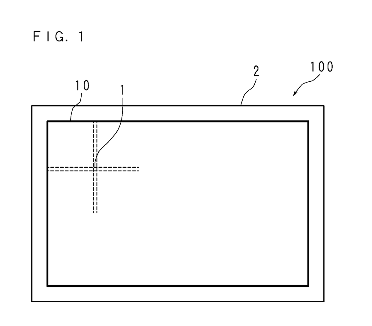
[0040]FIG. 1 is a front view schematically illustrating a liquid crystal panel 100 according to Embodiment 1. The liquid crystal panel 100 is a display panel, and is formed in a rectangular plate shape.

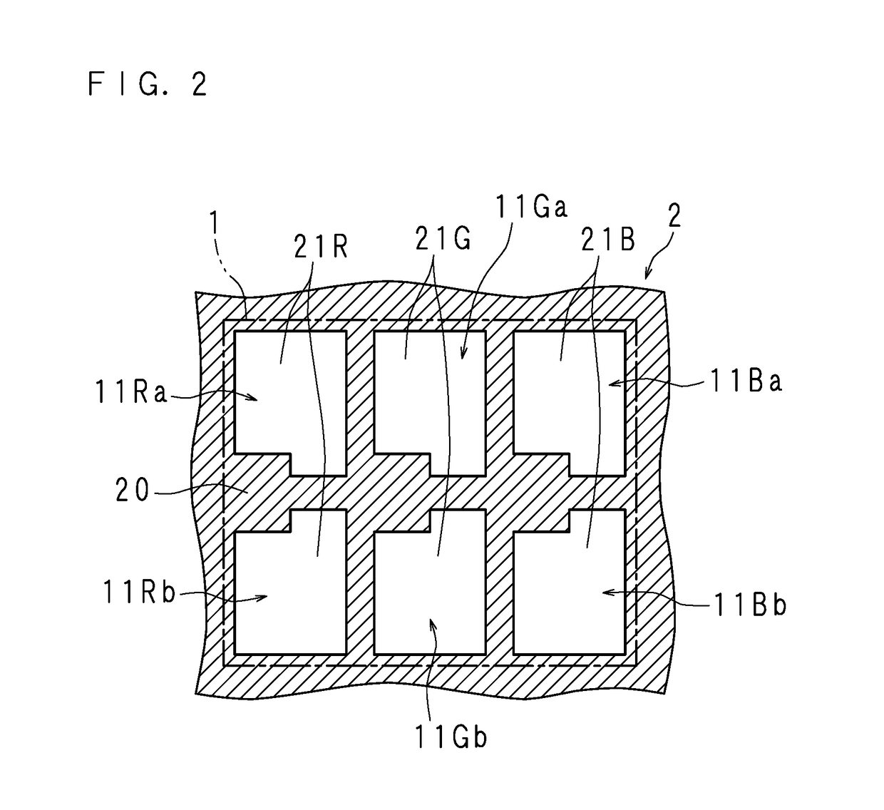
[0041]The liquid crystal panel 100 employs an active matrix type. The liquid crystal panel 100 has a pixel region 10 in which a plurality of pixels 1 are arranged in a matrix state as a lattice shape. For example, in the pixel region 10, 1920 pixels 1 and 1080 pixels 1 are aligned in a row direction and a column direction, respectively. Further, the pixels 1 according to Embodiment 1 includes six sub-pixels 11 as described below.

[0042]The liquid crystal panel 100 is constituted as described below. Color filters 21 are formed on a substrate 2 on a front side of the liquid crystal panel 100, of a pair of transparent rectangular substrates (glass substrates). The substrate 2 includes a transparent insulation film formed on the color filters 21, and further includes electrodes 22 formed t...

embodiment 2

[0078]In Embodiment 1, the configuration, in which the separated auxiliary capacitor control units 7 are connected to the unit wirings 71 and 72 of the groups I and II, or the unit wirings 73 and 74 of the groups III and IV, respectively, has been described. Compared with this, in Embodiment 2, a configuration, in which the number of the unit wirings is two times, and the separated auxiliary capacitor control units 7 are connected to unit wirings 71 to 74 of four groups I to IV, respectively, will be described.

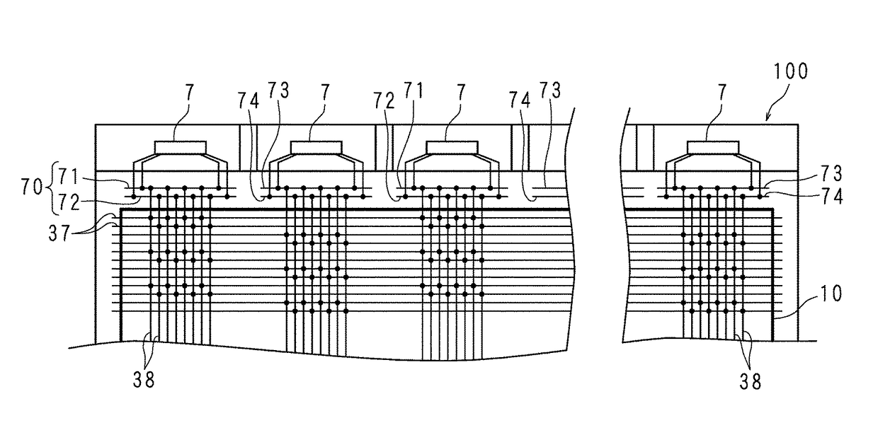
[0079]FIG. 7 is an explanatory view schematically illustrating an arrangement of a stem wiring 70 according to Embodiment 2. The stem wiring 70 is wired at the upper peripheral part outside the pixel region 10 along the row direction, so that two wirings thereof are separated into the same number. The separated wirings are referred to as the unit wirings 71 to 74, respectively. Further, the unit wirings 71 to 74 according to Embodiment 2 have a length half of that of the unit ...

embodiment 3

[0087]In Embodiments 1 and 2, the configuration in which the stem wiring 70 is disposed in the row direction, has been described. Compared with this, in Embodiment 3, a configuration, in which a stem wiring 70 is disposed in the column direction will be described.

[0088]FIG. 8 is an explanatory view schematically illustrating an arrangement of the stem wiring 70 according to Embodiment 3. The stem wiring 70 is wired at the peripheral part of both sides outside the pixel region 10 along the column direction, so that two wirings thereof are separated into the same number. The separated wirings are referred to as unit wirings 71 to 74, respectively. Further, FIG. 8 illustrates one side thereof in an enlarged form.

[0089]In response to outputting the control signal by the gate driver in block units obtained by dividing into a plurality of pixel regions 10 in the row direction, the auxiliary capacitor control unit 7 is similarly divided into block units. The auxiliary capacitor control uni...


PUM

PropertyMeasurementUnit
colorsaaaaaaaaaa
light intensitiesaaaaaaaaaa
transmissionaaaaaaaaaa

Abstract

Provided are a liquid crystal panel and a display apparatus using a liquid crystal panel preventing uneven luminance while contributing a slimmed border of the display apparatus.

Description

[0001]This application is the national phase under 35 U.S.C. 371 of PCT International Application No. PCT / JP2013 / 082156 which has an International filing date of Nov. 29, 2013 and designated the United States of America.BACKGROUND OF THE INVENTION[0002]1. Field of the Invention[0003]The present invention relates to a wiring structure in a driving circuit of a liquid crystal panel having a plurality of pixels disposed in a lattice shape therein. In particular, the present invention relates to a liquid crystal panel capable of efficiently achieving a prevention of display unevenness, while coping with a request of slimmed border in a display apparatus using the liquid crystal panel.[0004]2. Description of Related Art[0005]A display apparatus using a liquid crystal panel displays an image by allowing contrast to differ for each different position in the liquid crystal panel. Representation of the contrast is achieved by adjusting a transmission amount of light from a light source insta...

Claims


Application Information

Patent Timeline
Patent Type & Authority Patents(United States)
IPC IPC(8): G02F1/1362G02F1/1343
CPCG02F1/136213G02F1/136286G02F2001/134345G02F1/134345
Inventor YAMAMOTO, AKIHIROOHISHI, TAKUYA
Owner SAKAI DISPLAY PROD
Why Eureka
Try Eureka