Memory module with registers

a memory module and register technology, applied in the field of memory modules, can solve the problems of limiting signal integrity, difficult wiring of pins, and load of memory controllers, so as to avoid divergence of input signal ins, reduce mounting area, and preserve signal integrity

Active Publication Date: 2005-05-05
SAMSUNG ELECTRONICS CO LTD
View PDF7 Cites 10 Cited by
  • Summary
  • Abstract
  • Description
  • Claims
  • Application Information

AI Technical Summary

Benefits of technology

[0042] In this manner, pairs of registers are disposed to overlap on the front and back surfaces of the mounting module to reduce mounting area. In addition, the input signal INS is transferred through the registers in series as a daisy chain to avoid divergence of the input signal INS for preserving signal integrity.
[0043] Furthermore, because each of the registers has reduced pins, area for wiring is in turn reduced. Additionally, each of the registers buffers the input signal INS to corresponding semiconductor banks that are closely disposed to the sides of the register for further reduced wiring area. With reduced mounting area and reduced wiring area, more memory chips may be included for larger capacity of the memory module.

Problems solved by technology

Also, since a memory controller must transmit signals to each of the registers, a higher number of registers increases the load of the memory controller thus limiting signal integrity.
Also, as the number of pins of the first and second registers RF and RR increases, wiring of the pins becomes more difficult, and additional space for the wiring is required.
Unfortunately, signal integrity is diminished from impedance mismatching with such T-shaped divergence of the input signal INS.

Method used


Image

  • Memory module with registers
  • Memory module with registers
  • Memory module with registers

Examples


Embodiment Construction

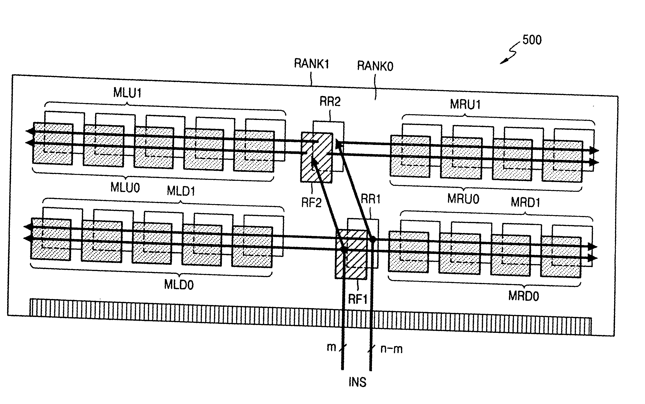
[0052]FIG. 5 illustrates a memory module 500 according to an embodiment of the present invention. FIG. 6 is a signal connection diagram of the memory module of FIG. 5.

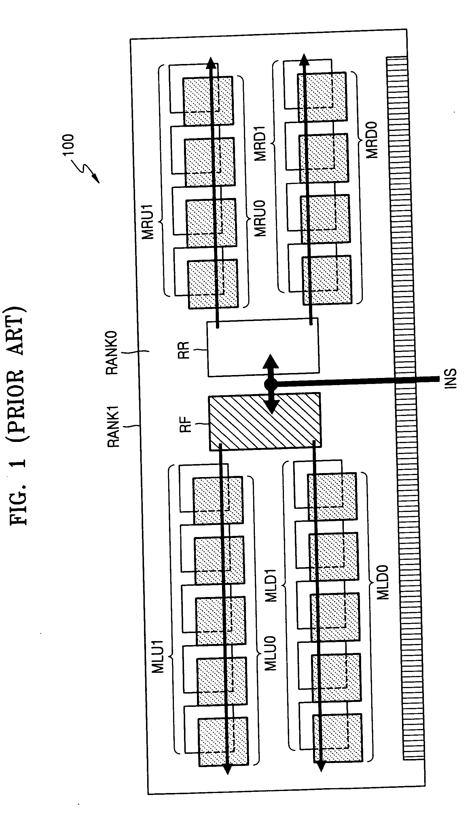
[0053] Referring to FIG. 5, a memory module 500 includes memory banks MLD0, MLU0, MRD0 and MRU0 mounted on a front surface RANK0 of the memory module 500 and includes memory banks MLD1, MLU1, MRD1 and MRU1 mounted on a back surface RANK1 of the memory module 500.

[0054] A memory bank referred to by MLD0, MLU0, MRD0, MRU0, MLD1, MLU1, MRD1 or MRU1 is defined broadly herein just as a group of at least one memory chip. The memory module 500 is a dual in line memory module (DIMM) that includes memory chips on both of the front and back surfaces RANK0 and RANK1.

[0055] The memory module 500 also includes first, second, third, and fourth registers, RF1, RF2, RR1, and RR2, respectively. The registers RF1 and RR1 comprising a first pair are mounted on the front surface RANK0 and the back surface RANK1, respectively, of the me...


PUM


Abstract

Pairs of registers with reduced pins are disposed to overlap on front and back surfaces of a memory module. An input signal INS is transferred through the registers in series in a daisy chain fashion to avoid divergence of the input signal INS for preserved signal integrity. Each register buffers the input signal INS to memory banks disposed closely to sides of the register for reduced wiring area.

Description

[0001] This application claims priority to Korean Patent Application No. 2003-0076734, filed on Oct. 31, 2003, in the Korean Intellectual Property Office, the disclosure of which is incorporated herein in its entirety by reference. BACKGROUND OF THE INVENTION [0002] 1. Field of the Invention [0003] The present invention relates generally to memory modules, and more particularly, to a memory module having registers mounted with minimized area and with preservation of signal integrity. [0004] 2. Description of the Related Art [0005] A memory module includes registers that receive signals from external devices and transfer such signals to memory chips mounted in the memory module. If the number of memory chips in a memory module is large, the memory module typically includes a plurality of registers. [0006] A number of output pins of each of the registers for connecting to memory chips decreases with higher number of registers for improved signal integrity. On the other hand, a larger ...

Claims


Application Information

Patent Timeline
Patent Type & Authority Applications(United States)
IPC IPC(8): G06F12/00G06F12/06G06F13/16G11C5/00H01L23/50
CPCG11C5/04H01L23/50
Inventor PARK, KWANG-SOOCHO, JEONG-HYEONSO, BYUNG-SELEE, JUNG-JOONYUN, YOUNGKIM, KWANG-SEOP
Owner SAMSUNG ELECTRONICS CO LTD
Why Eureka
Try Eureka