
Power MOSFET having improved manufacturability, low on-resistance and high breakdown voltage

a technology of power mosfet and superjunction mosfet, which is applied in the direction of semiconductor devices, semiconductor/solid-state device details, electrical equipment, etc., can solve the problems of high volume, high cost, and inability to manufacture the superjunction mosfet of fig. 1 type, and achieve the effect of reducing the drain-to-source resistan

Active Publication Date: 2017-12-05
LITTELFUSE INC
View PDF2 Cites 0 Cited by
  • Summary
  • Abstract
  • Description
  • Claims
  • Application Information

AI Technical Summary

Benefits of technology

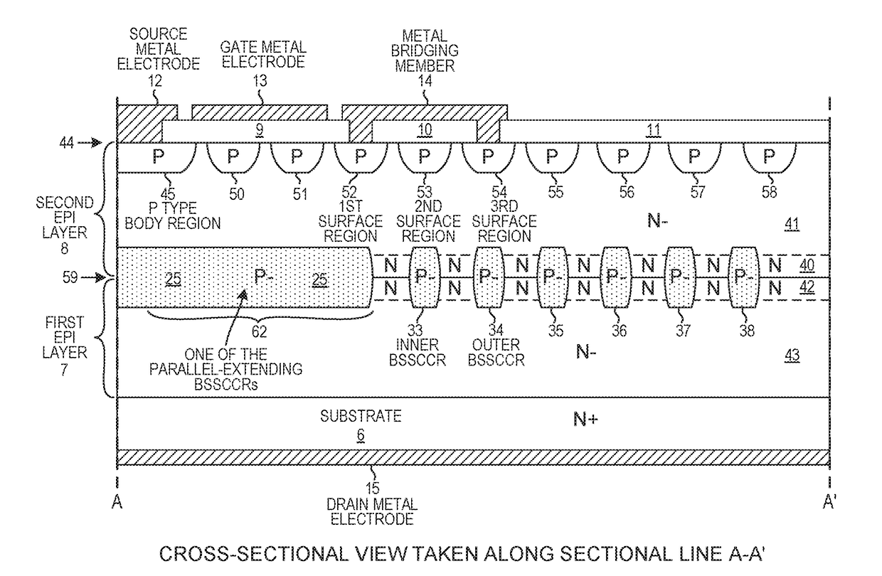
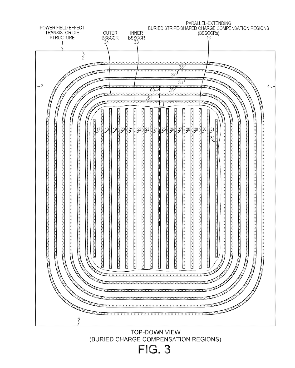
This patent describes a new design for a power field effect transistor (PFET) that has a high breakdown voltage rating. The design includes a floating P type surface ring structure and three concentric P type surface rings. The breakdown voltage rating is achieved by reducing the electric field in the vicinity of the buried inner P type BSSCCRs. The PFET has a unique structure with two and only two epitaxial layers, which allows for simplified processing. The design also reduces current crowding and RDS(ON) of the device by shaping the BSSCCRs with a cross-sectional height greater than its width. The resulting device has a cross-sectional height that is greater than its cross-sectional width, which further enhances its performance.

Problems solved by technology

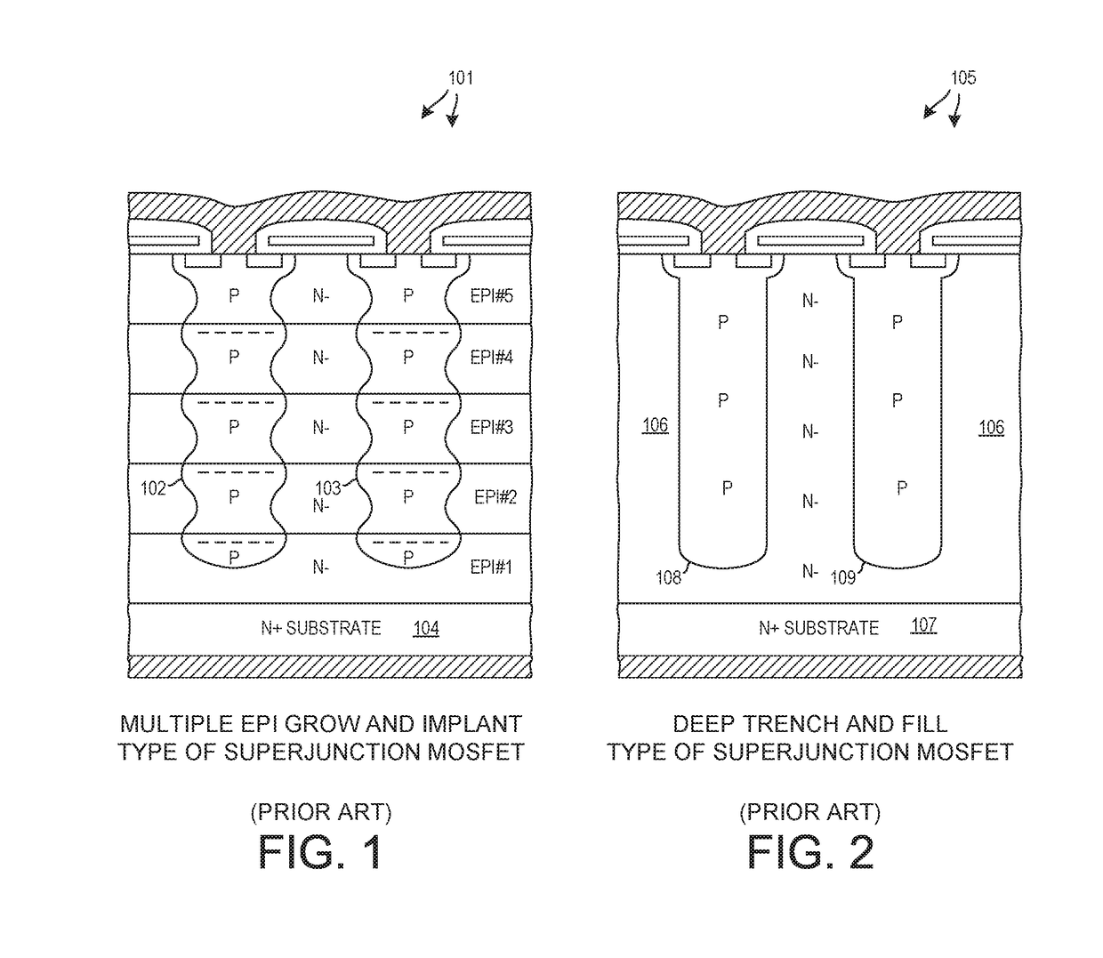
Equipment and expertise to perform the deep trench etching required to the make the device of FIG. 2 is lacking in some such semiconductor fabs.
In high volume semiconductor fabs that typically make digital logic devices in high volume, the manufacturing of the type of superjunction MOSFET of FIG. 1 is typically not possible because these fabs do not typically have equipment to grow the epitaxial silicon layers.
The importing of items into the high volume and expensive facility is a source of impurities and contamination that can disrupt other operations of the facility.
The operators of such facilities may, therefore, decline to manufacture power devices of the type of FIG. 1 in relatively low volumes because doing so would involve importing unfinished wafers into the plant over and over as each successive one of the epitaxial layers that was deposited outside the fab is brought back into the fab so that the next implanting step can be done.
Accordingly, due to the limitations on where devices involving many epitaxial layers can be made, fabrication costs associated with the superjunction MOSFET of FIG. 1 can be undesirably high.

Method used


Image

  • Power MOSFET having improved manufacturability, low on-resistance and high breakdown voltage
  • Power MOSFET having improved manufacturability, low on-resistance and high breakdown voltage
  • Power MOSFET having improved manufacturability, low on-resistance and high breakdown voltage

Examples


Embodiment Construction

[0030]Reference will now be made in detail to some embodiments of the invention, examples of which are illustrated in the accompanying drawings. In the description and claims below, when a first object is referred to as being disposed “over” or “on” a second object, it is to be understood that the first object can be directly on the second object, or an intervening object may be present between the first and second objects. Similarly, terms such as “upper”, “top”, “up”, “on”, “over”, “cover”, “down”, “vertical”, “horizontal”, “laterally”, “lower”, “bottom”, “underneath”, “height” and “width” are used herein to describe relative orientations between different parts of the structure being described, and it is to be understood that the overall structure being described can actually be oriented in any way in three-dimensional space. The notations N+, N, N−, P, and P− are only relative, and are to be considered in context, and do not denote any particular dopant concentration range.

[0031...


PUM


Abstract

Stripe-shaped surface transistor structures of a power MOSFET are disposed over an array of parallel-extending P type Buried Stripe-Shaped Charge Compensation Regions (BSSCCRs). The power MOSFET has two and only two epitaxial semiconductor layers, and the BSSCCRs are disposed at the interface between these layers. Looping around the area occupied by these parallel-extending BSSCCRs is a P type ring-shaped BSSCCR. At the upper semiconductor surface are disposed three P type surface rings. The inner surface ring and outer surface ring are coupled together by a bridging metal member, but the center surface ring is floating. The bridging metal member is disposed at least in part over the ring-shaped BSSCCR. The MOSFET has a high breakdown voltage, a low RDS(ON), and is acceptable and suitable for manufacture at semiconductor fabrication plants that cannot or typically do not make superjunction MOSFETs.

Description

TECHNICAL FIELD[0001]The described embodiments relate to power field effect transistor devices.BACKGROUND INFORMATION[0002]For the same breakdown voltage (BVDSS) rating and the same die size, the drain-to-source on-resistance (RDS(ON)) of a so-called “superjunction” field effect transistor (also called a “superjunction MOSFET”) will generally be lower than the RDS(ON) of a conventional non-superjunction MOSFET device. For this reason, superjunction MOSFETs are taking a larger and larger share of the overall MOSFET market as compared to the share attributed to conventional trench-type and planar-type MOSFETs.[0003]FIG. 1 (Prior Art) is a simplified cross-sectional diagram of one type of superjunction MOSFET 101. The vertically oriented charge-balancing pillar structures 102 and 103 of P type semiconductor material are formed by depositing an N− type epitaxial semiconductor layer EPI#1 on an N+ type wafer substrate 104. Regions of P type dopants are implanted into the top surface of E...

Claims


Application Information

Patent Timeline
Patent Type & Authority Patents(United States)
IPC IPC(8): H01L29/78H01L29/10H01L29/06H01L29/08H01L23/535H01L29/417
CPCH01L29/7811H01L29/1079H01L29/0692H01L29/0634H01L29/0856H01L23/535H01L29/41741H01L29/1095H01L29/0623H01L29/7813H01L23/4824H01L29/0878H01L29/0619
Inventor SEOK, KYOUNG WOOK
Owner LITTELFUSE INC
Learn More