
Infrared image sensor

a technology of infrared image and sensor, which is applied in the direction of optical radiation measurement, radiation control devices, instruments, etc., can solve the problems of image visibility degradation of the sensor, and achieve the effect of improving image visibility and minimizing dark currents

Active Publication Date: 2017-12-19
SILICON DISPLAY TECH CO LTD
View PDF7 Cites 1 Cited by
  • Summary
  • Abstract
  • Description
  • Claims
  • Application Information

AI Technical Summary

Benefits of technology

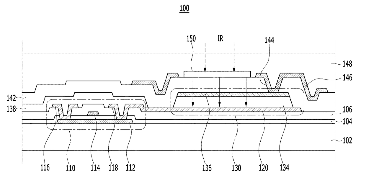
This patent describes an image sensor that can improve visibility by converting infrared rays into visible ones using a semiconductor material that operates in the visible ray wavelength band. The sensor can also minimize dark currents without using an additional cooling process.

Problems solved by technology

However, semiconductor materials used to absorb light of an infrared wavelength band in an infrared image sensor have small bandgaps, and thus a dark current may be generated by thermally excited electrons.
This dark current acts as noise in the image sensor, and thus an image visibility of the sensor may be deteriorated.

Method used


Image

  • Infrared image sensor
  • Infrared image sensor
  • Infrared image sensor

Examples


Embodiment Construction

[0043]The present invention will be described more fully hereinafter with reference to the accompanying drawings, in which exemplary embodiments of the invention are illustrated. As those skilled in the art would realize, the described embodiments may be modified in various different ways, all without departing from the spirit or scope of the present invention. Accordingly, the drawings and description are to be regarded as illustrative in nature and not restrictive, and like reference numerals designate like elements throughout the specification. Further, detailed description of a well-known related art will be omitted.

[0044]In the drawings, the thickness of layers, films, panels, regions, etc., are exaggerated for clarity. It will be understood that when an element such as a layer, film, region, or substrate is referred to as being “on” another element, it can be directly on the other element or intervening elements may also be present. In the meantime, when an element is referred...


PUM


Abstract

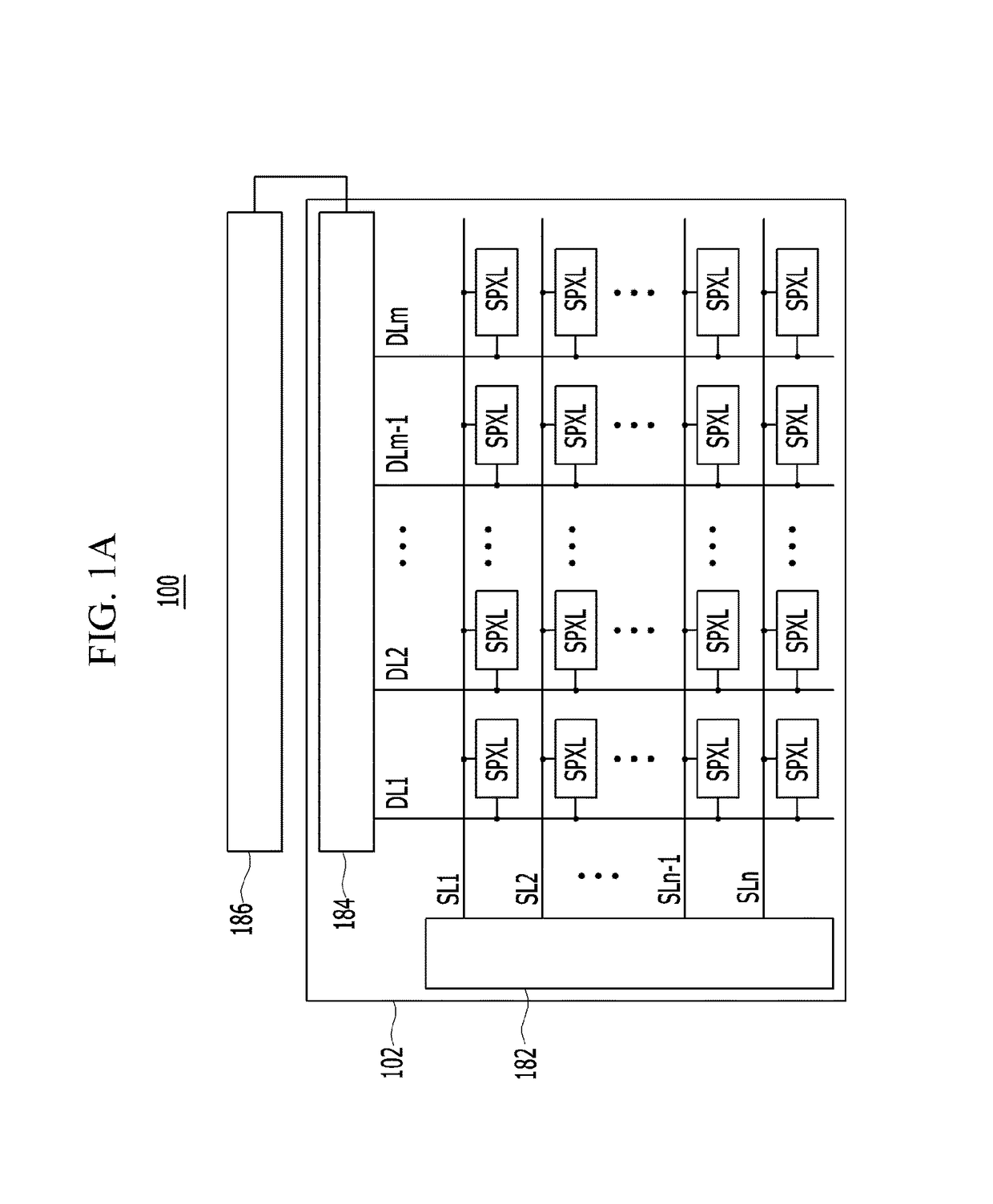
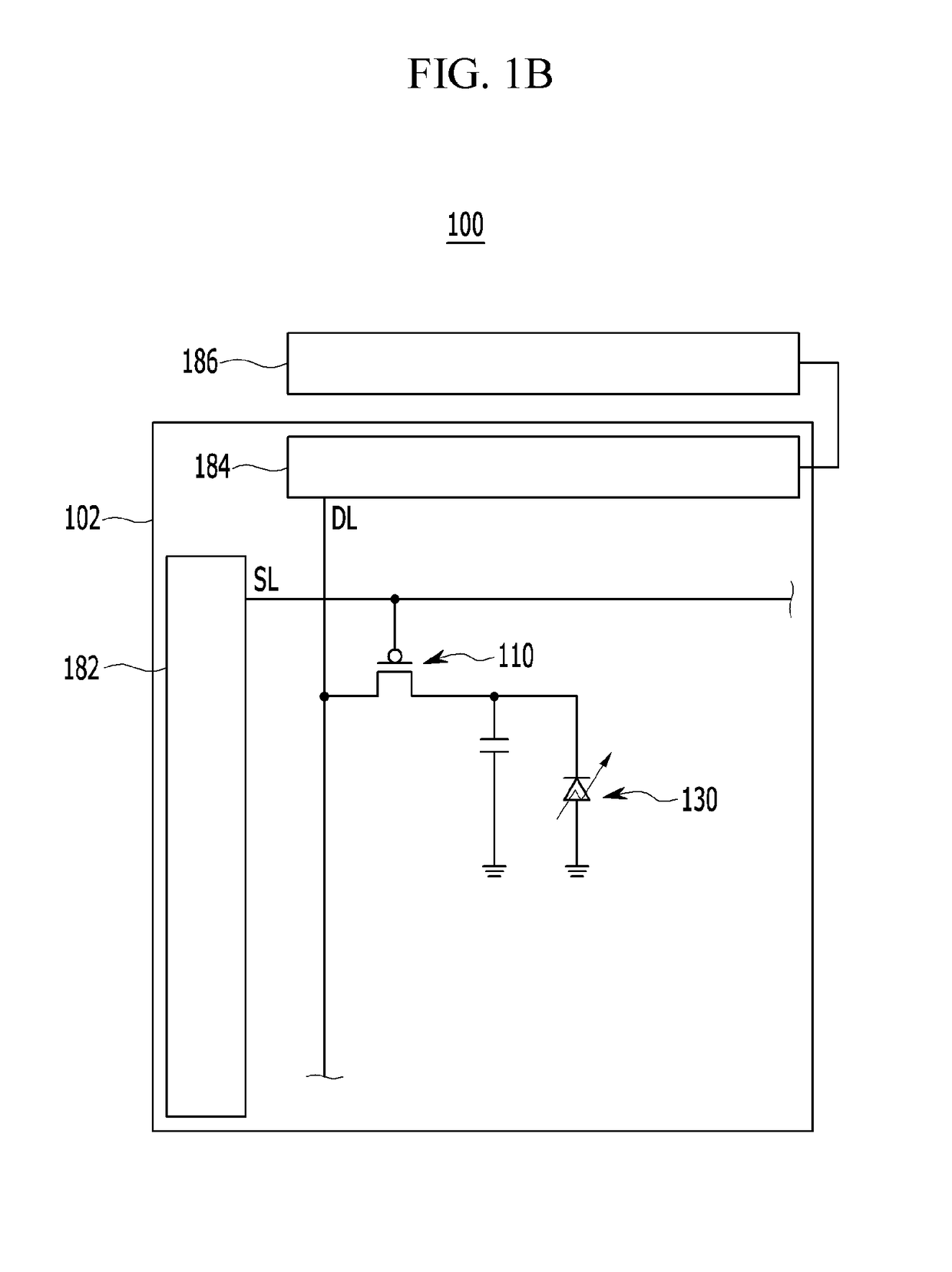
An exemplary embodiment of the present invention provides an infrared image sensor including: a sensor pixel connected with a data lead-out line and a scan line disposed on a surface of a substrate; a wavelength converter positioned in the sensor pixel and disposed in an internal movement path of infrared rays, including an anti-Stokes material that absorbs infrared rays and converts them into visible rays to emit them; and a photosensor part positioned in the sensor pixel to sense the visible rays converted by the wavelength converter.

Description

CROSS-REFERENCE TO RELATED APPLICATION[0001]This application claims priority to and the benefit of Korean Patent Application No. 10-2016-0170559 filed in the Korean Intellectual Property Office on Dec. 14, 2016, the entire contents of which are incorporated herein by reference.BACKGROUND OF THE INVENTION(a) Field of the Invention[0002]This relates to an infrared image sensor.(b) Description of the Related Art[0003]An image sensor is a device that acquires an image by using a property of a semiconductor to react with light. Recently, with development of computer industries and communication industries, image sensors having improved performance in various fields such as digital cameras, scanners, camcorders, personal communication systems (PCS), game devices, light cameras, and medical micro cameras have been used.[0004]In Korean Patent Publication No. 10-2016-0036249 relating to an image sensor using infrared rays, the image sensor disclosed therein includes: a backlight unit; a visi...

Claims


Application Information

Patent Timeline
Patent Type & Authority Patents(United States)
IPC IPC(8): H01L27/14G01J1/42H01L27/30H01L27/146G01J1/58
CPCH01L27/14649H01L27/14625H01L27/14607H01L27/14636H01L27/14629H01L27/307H01L27/14616G01J1/4228G01J1/58H10K39/32G01J5/48H01L27/146H01L27/14612H04N5/33
Inventor KIM, JAEMINKIM, KIJOONGYU, JIN HYEONGHUR, JI HO
Owner SILICON DISPLAY TECH CO LTD
Learn More