Antenna laminate and image display device including the same
a technology of image display device and antenna, which is applied in the direction of resonant antennas, protective materials radiating elements, instruments, etc., can solve the problems of difficult to secure an appropriate mounting space, electrical characteristics of the antenna, touch sensor, display panel disturbance, etc., to improve the signal characteristics of the antenna (antenna gain and efficiency, space utilization may be improved, and the effect of decreasing the thickness of the antenna
- Summary
- Abstract
- Description
- Claims
- Application Information
AI Technical Summary
Benefits of technology
Problems solved by technology
Method used
Image
Examples
examples 1 to 8
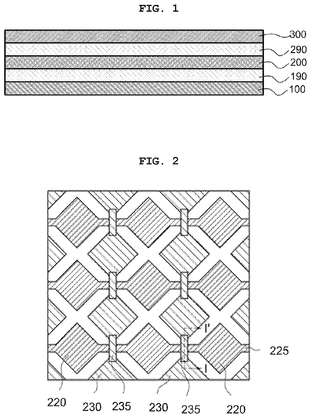
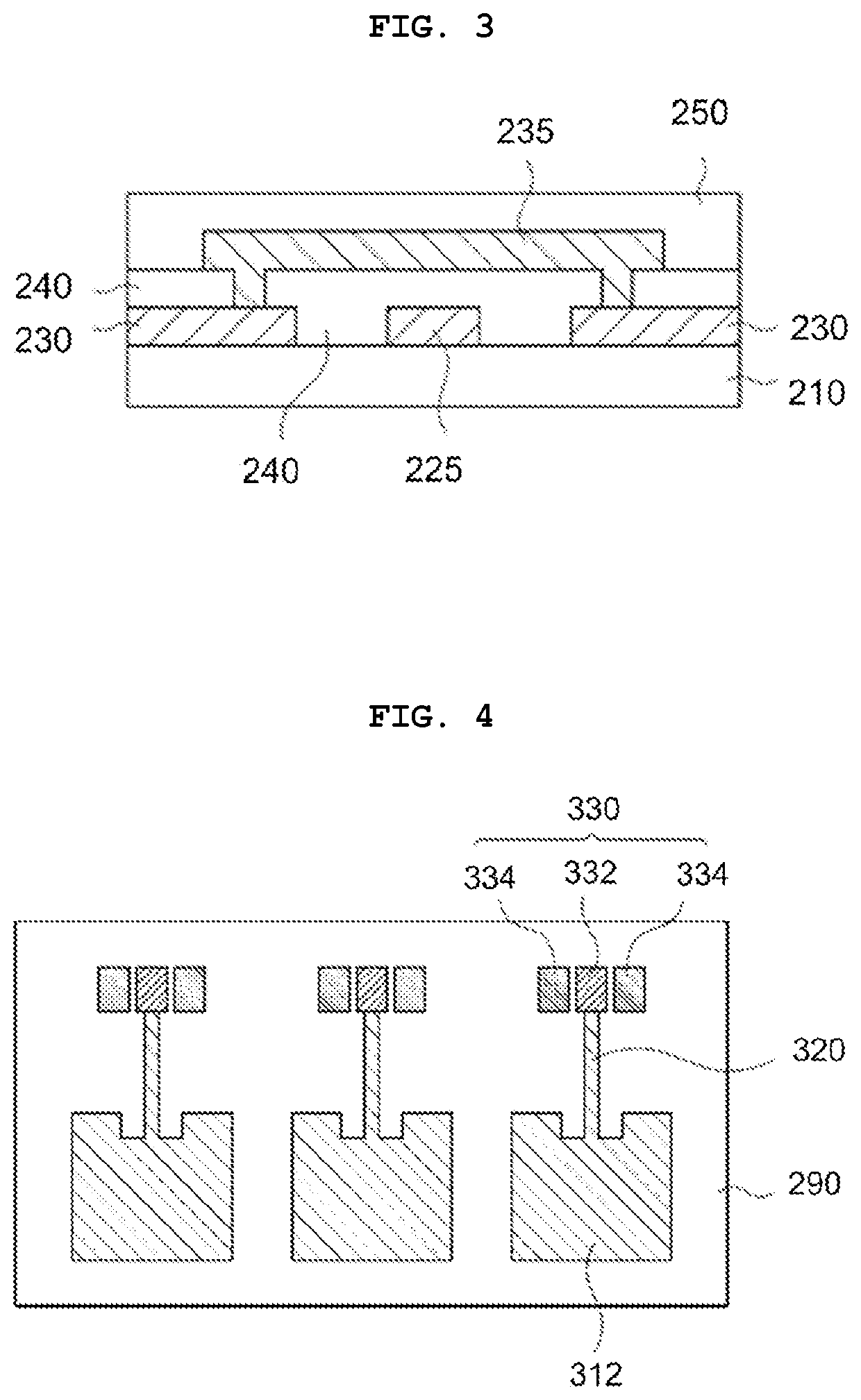
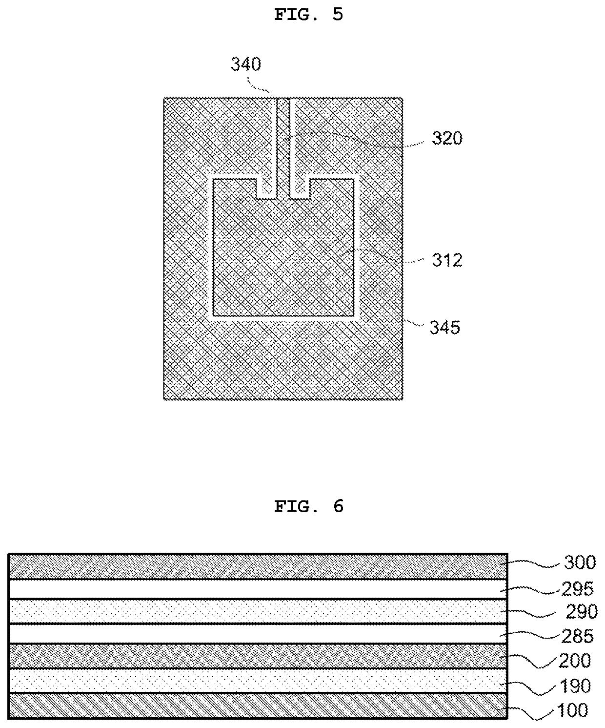
[0121]An antenna electrode layer was formed on an upper surface of a polyimide dielectric layer using a silver-palladium-copper (APC) alloy.
[0122]Then, a touch electrode layer including sensing electrodes made of indium tin oxide (ITO) having a thickness of 3 to 4 μm was adhered below the dielectric layer.
[0123]A distance between the antenna electrode layer and the touch electrode layer was adjusted to 400 μm.
[0124]A lower surface of the touch electrode layer was adhered to an OLED panel to prepare an image display device.
[0125]Distances between the touch electrode layer and the electrode structure (a TFT electrode and a pixel electrode) of the OLED panel were adjusted as shown in Table 1 below.
experimental example
Characteristics of Antenna
[0129]S-parameters (S11, return losses) and antenna efficiencies were extracted from the image display devices and the antenna laminate prepared in the examples and comparative example at a frequency of about 27.5 to 28.5 GHz with an impedance of 50Ω using a network analyzer, and results thereof are shown in Table 1 below.
[0130]
TABLE 1Distance betweentouch electrode layerand electrode structureof OLED panelS11Efficiency(μm)(dB)(%)Example 110−9.0887.1Example 225−9.1087.2Example 350−9.4788.7Example 4100−7.8283.5Example 5150−7.0280.2Example 6240−4.5364.8Example 7380−4.0160.3Example 8480−3.4154.4ComparativeOLED panel−3.4053.3Example 1(none)
[0131]Referring to Table 1, it can be seen that antenna performances of the examples were improved compared to those of the comparative example which does not include the OLED panel used as the second ground layer in the examples.
reference examples 1-9
[0132]An antenna electrode layer made of a silver-palladium-copper (APC) alloy was disposed on a polyimide dielectric layer, and a ground layer made of an APC alloy (‘APC ground layer’) having a thickness of 2400 Å was formed below the dielectric layer. A resistance of the APC ground layer was 0.15 kW.
[0133]Antenna characteristics were evaluated in the same manner as the experimental example while adjusting the thicknesses of the dielectric layers as shown in Table 2 below.
[0134]
TABLE 2Thickness ofdielectricRadiationlayerEfficiencyGainDirectivity(μm)(%)(dBi)(dBi)Reference100.13−28.237.72Example 1Reference500.45−15.488.04Example 2Reference100180.147.54Example 3Reference20043.73.27.32Example 4Reference30064.35.357.27Example 5Reference40078.05.67.18Example 6Reference50080.36.187.14Example 7Reference700856.357.07Example 8Reference100087.86.156.8Example 9
[0135]Referring to Table 2, it can be seen that the antenna efficiencies and gains of the reference examples were increased as the thic...
PUM
| Property | Measurement | Unit |
|---|---|---|
| thickness | aaaaa | aaaaa |
| thickness | aaaaa | aaaaa |
| dielectric constant | aaaaa | aaaaa |
Abstract
Description
Claims
Application Information


