Arrangement for a touchscreen and related method of manufacture

a touchscreen and display device technology, applied in the field of optical and electronic devices, can solve the problems of unsatisfactory, traditional touchscreens are often somewhat pricey to implement and manufacture, and the sealing between them and the finger is not per

Active Publication Date: 2018-01-09
TACTOTEK
View PDF37 Cites 1 Cited by
  • Summary
  • Abstract
  • Description
  • Claims
  • Application Information

AI Technical Summary

Benefits of technology

[0040]As alluded hereinbefore, the utility of the different aspects of the present invention arises from a plurality of issues depending on each particular embodiment. The manufacturing costs for producing the touch screen arrangement in accordance with the present invention may be kept low due to rather extensive use of affordable and easily obtainable materials, components, and process technology. The feasible process technology also enables rapid industrial scale manufacturing of the arrangement in addition to mere prototyping scenarios. The arrangement may be kept thin, light, and energy conserving in order to suit most use scenarios with little modifications to the surrounding elements and designs. The coupling losses between the emitters, lightguide, and the detectors may be minimized as external, typically lossy, light funneling means such as gratings etc. are not necessary. The touch detection capability of the various embodiments of the arrangement is good with low sensitivity to e.g. dirt on the touch surface, and even multi-touch applications may be constructed. The arrangement may be easily combined with an existing display or device layout, and conveniently connected to an external target entity such as a host device mainboard via a flex cable, for example, which also enables easy replacement thereof in the future. The arrangement may further be made robust towards external impacts, depending on the used materials, in which case the arrangement also function as an optionally replaceable screen cover for the underlying display element. Yet, the arrangement suits particularly well various industrial applications including e.g. industrial automation / electronics control apparatuses, as it may provide hermetical (˜splash-proof) isolation from the hostile use environment like humid and / or dusty air. The embodiments of the invention may be utilized in various hand-held devices, wristop devices, gaming devices, household appliances, sports devices, and automotive products, for instance.

Problems solved by technology

In practice, e.g. the surface roughness of the lightguide affects the fact that the sealing between it and the finger, which has surface irregularities as well, is not perfect, i.e. some air still remains in between.
Without any intention to deny the advantages and benefits offered by currently available touchscreen or corresponding solutions in providing more sophisticated UI means over more conventional options such as keyboards and mouses, certain problems still exist therewith naturally depending on each particular use case.
For example, traditional touchscreens are often somewhat pricey to implement and manufacture, and they also take a considerable amount of space in the end product without forgetting the induced additional weight, which must be thus taken into account in the very beginning of the overall R&D project.
The touchscreens may even consume surprising amount of extra power e.g. in the context of mobile devices.
Such structures require some more design work and may add to the end product weight, coupling losses, and price among other factors.

Method used


Image

  • Arrangement for a touchscreen and related method of manufacture
  • Arrangement for a touchscreen and related method of manufacture
  • Arrangement for a touchscreen and related method of manufacture

Examples


Embodiment Construction

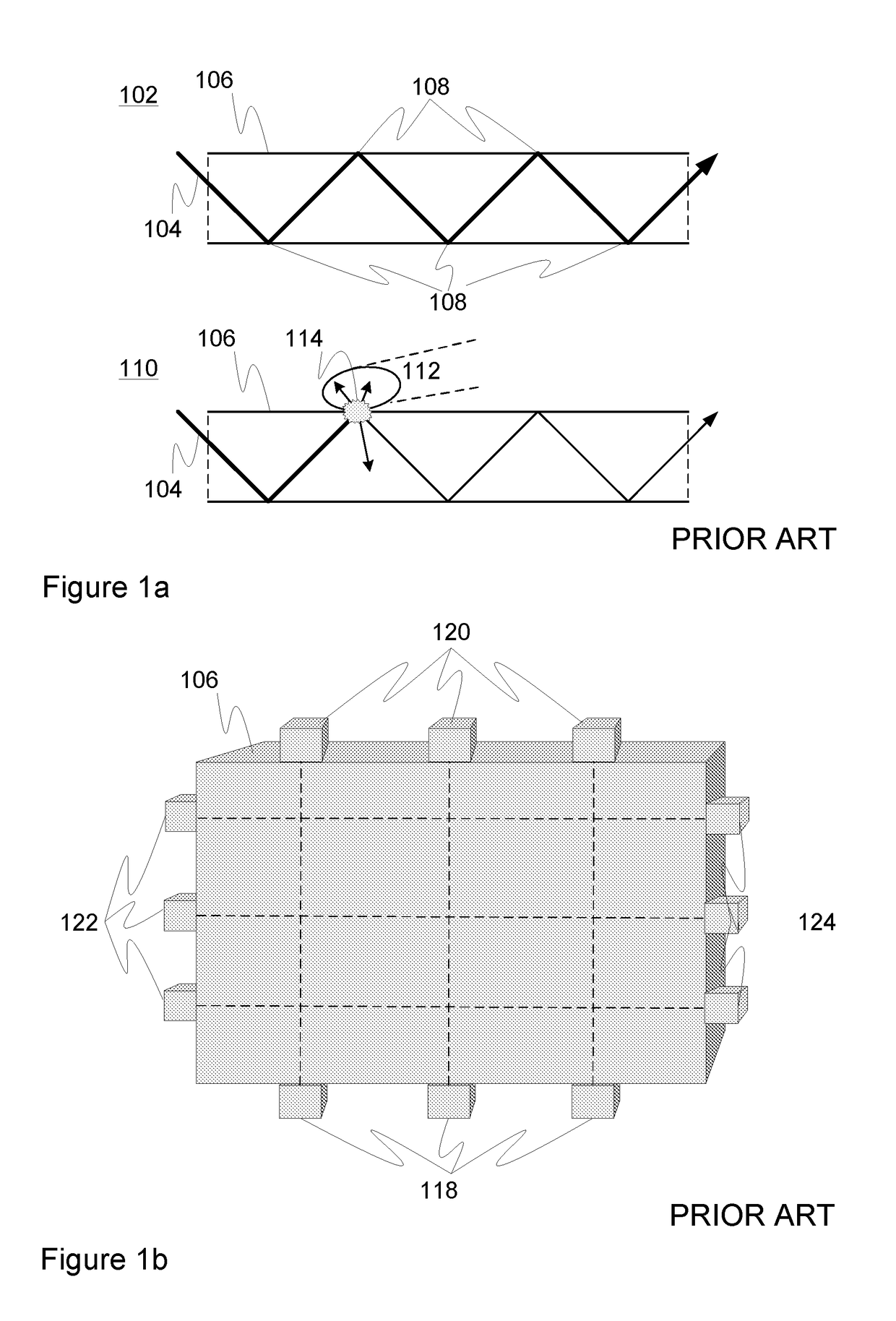
[0057]FIGS. 1a and 1b were already contemplated hereinbefore in connection with the review of the background of the invention.

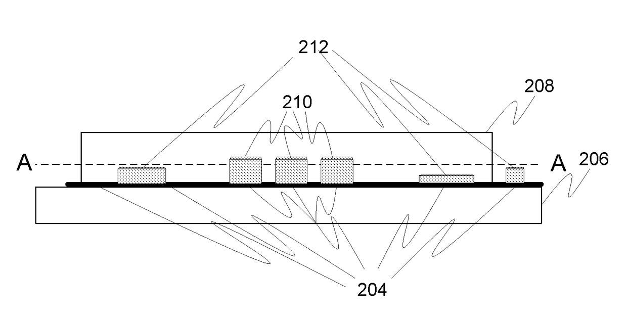
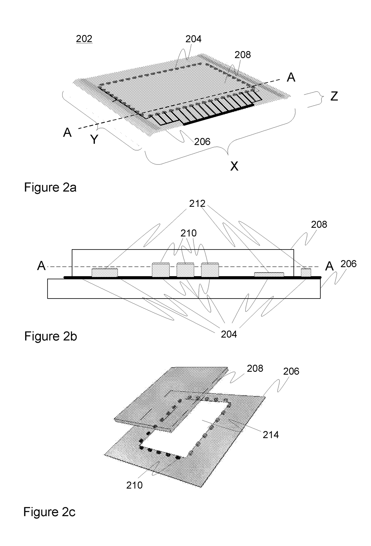
[0058]Now referring to FIG. 2a, a perspective view 202 of one embodiment of the touch-screen arrangement is sketched. The touchscreen arrangement, which may be implemented as an overlay for a display, comprises a substrate such as a (flexible) film 206 accommodating electronics 204 such as support electronics like conductors and / or control circuitry, and also further electronic elements such as optoelectronic light emitter(s), detector(s), and optionally other components. The lightguide 208 has been provided thereon.

[0059]For example, in-mould integration may be applied such that the lightguide material is over-moulded onto the electronics on the substrate, wherein the substrate provided with the electronics is used as an in-mould insert in the injection moulding process. As a result, the over-moulded material acts as a lightguide between the emitters and the...


PUM

PropertyMeasurementUnit
critical angleaaaaaaaaaa
refractive indexaaaaaaaaaa
transmittanceaaaaaaaaaa

Abstract

Arrangement for use with a touchscreen, includes a substrate, such as an optically substantially transparent film or a film defining a through hole, the substrate including support electronics, such as printed electronics including a number of printed conductors, for providing power, control and / or communications connection to further electronic components, a number of emitters and detectors arranged on the substrate into contact with the support electronics, for emitting and detecting light, respectively, and a lightguide arranged onto the substrate such that the emitters and detectors, and optionally at least part of the support electronics, are substantially immersed in the lightguide material, the properties of the lightguide including the refractive index of the lightguide material being selected and the emitters and detectors being configured so as to enable, when in use, total internal reflection (TIR)-type propagation of light within the lightguide between the emitters and detectors and recognition of a touch on the basis of a drop in the TIR performance as determined from the detected light. A related method of manufacture is presented.

Description

FIELD OF THE INVENTION[0001]Generally the invention relates to optics and electronics. Particularly, however not exclusively, the invention pertains to UIs (user interface) comprising a touchscreen arrangement utilizing the total internal reflection (TIR) phenomenon.BACKGROUND[0002]Concerning contemporary and future electronic appliances for both consumer and professional use, the importance of a decent UI and usability in general cannot be stressed too much. In addition to conventional keypad, keyboard, or button arrangements, different kinds of touchscreens have been developed to provide the users of the appliances with more instant and versatile way of controlling the related applications.[0003]Touchscreens may apply of a number of varying technologies for obtaining the touch-sensitive functionality. Among various other potential options e.g. capacitive, resistive, infrared, optical imaging (camera-based), acoustic, and hybrid solutions are feasible.[0004]Some infrared solutions ...

Claims


Application Information

Patent Timeline
Patent Type & Authority Patents(United States)
IPC IPC(8): G06F3/041F21V8/00G06F3/042
CPCG02B6/0065G02B6/0021G06F3/0421Y10T29/49146G06F2203/04109Y10T29/4913G02B6/0083G06F3/041
Inventor AIKIO, JANNEKERANEN, ANTTI
Owner TACTOTEK
Why Eureka
Try Eureka