Eureka AIR delivers breakthrough ideas for toughest innovation challenges, trusted by R&D personnel around the world.

FinFET-based ESD devices and methods for forming the same

Active Publication Date: 2018-02-13
TAIWAN SEMICON MFG CO LTD
View PDF35 Cites 0 Cited by
  • Summary
  • Abstract
  • Description
  • Claims
  • Application Information

AI Technical Summary

Benefits of technology

The patent text describes a method for making a FinFET-based Electrostatic Discharge (ESD) device and its use in integrated circuits. The technical effects of the patent include providing a more effective way to protect integrated circuits from ESD damage, which can be caused by static charges, and the design and process issues that arise when incorporating ESD devices into FinFET structures. The method involves incorporating ESD devices into FinFET structures to provide high ESD protection capability. The breakdown of any one of the FinFET devices can cause malfunction of the entire ESD protection circuit, so the FinFET devices need to be turned on uniformly. The patent also discusses various methods for forming the ESD device, including the use of metal layers and vias to electrically couple source and drain epitaxy regions of the ESD device. The patent also mentions the applications in which a FinFET-based ESD device may be used. Overall, the patent provides a solution for effectively protecting integrated circuits from ESD damage and improving the design and process of ESD devices in FinFET structures.

Problems solved by technology

Extremely high voltages can develop in the vicinity of integrated circuits due to the build-up of static charges.
ESD is a serious problem for semiconductor devices since it can potentially destroy the entire integrated circuit.
The duration of the ESD transient is very short, typically in the order of nanoseconds, and the conventional circuit breakers cannot react quickly enough to provide adequate protection.

Method used


Image

  • FinFET-based ESD devices and methods for forming the same
  • FinFET-based ESD devices and methods for forming the same
  • FinFET-based ESD devices and methods for forming the same

Examples


Embodiment Construction

[0011]The making and using of the embodiments of the disclosure are discussed in detail below. It should be appreciated, however, that the embodiments provide many applicable inventive concepts that can be embodied in a wide variety of specific contexts. The specific embodiments discussed are illustrative, and do not limit the scope of the disclosure.

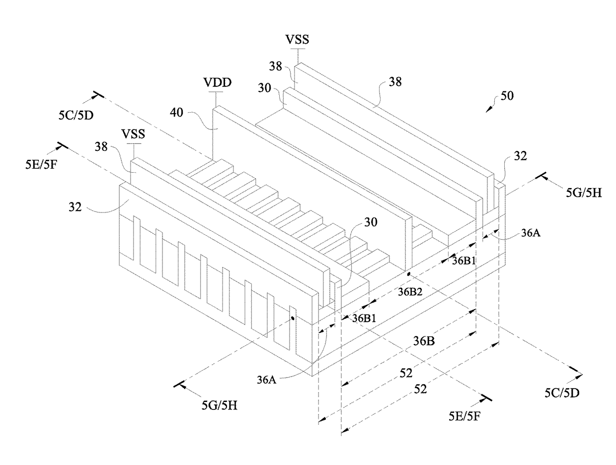
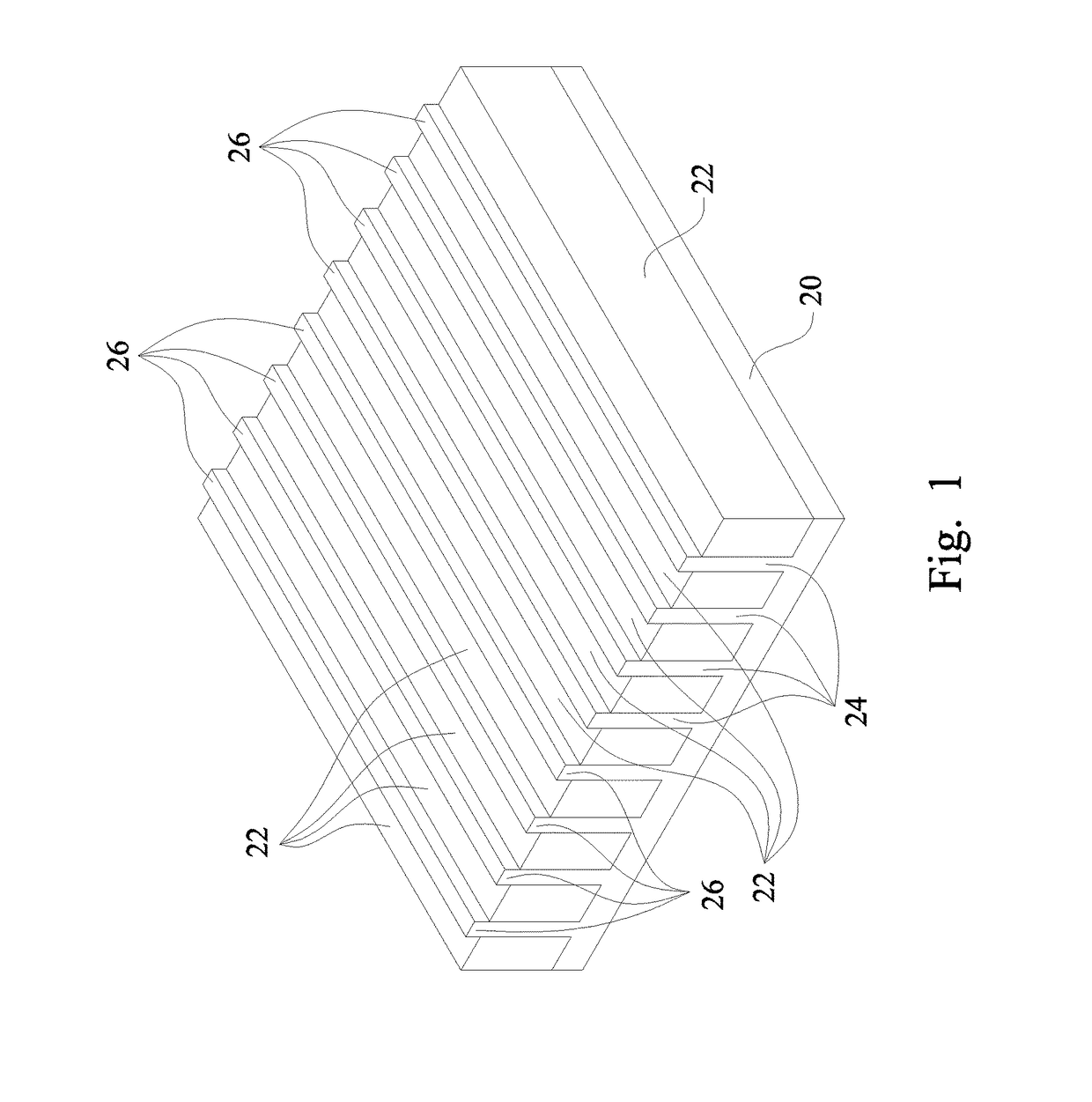
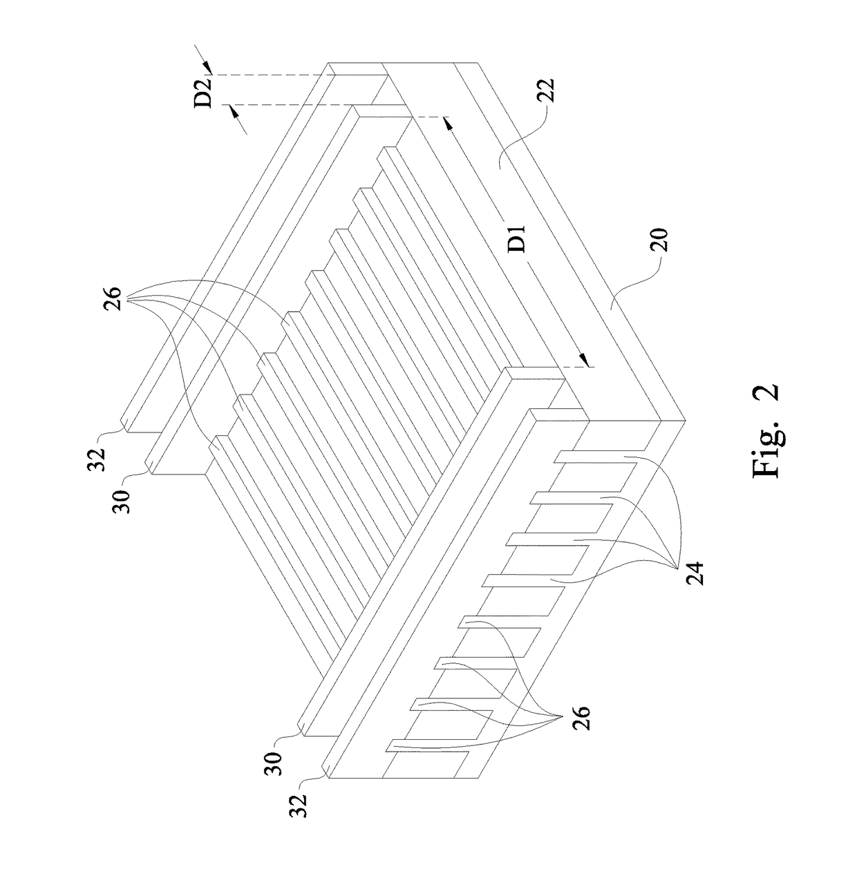
[0012]A Fin Field-Effect Transistor (FinFET) based ElectroStatic Discharge (ESD) device and the methods of forming the same are provided in accordance with various exemplary embodiments. Intermediate stages of forming the ESD device are illustrated. Some variations of the embodiments are discussed. Additionally, some applications in which a FinFET based ESD device may be used are also discussed. Throughout the various views and illustrative embodiments, like reference numbers are used to designate like elements.

[0013]FIGS. 1 through 5H illustrate perspective views, top views, and cross-sectional views of intermediate stages in the forma...


PUM


Abstract

A semiconductor device includes semiconductor fins on semiconductor strips on a substrate. The semiconductor fins are parallel to each other. A gate stack is over the semiconductor fins, and a drain epitaxy semiconductor region is disposed laterally from a side of the gate stack and on the semiconductor strips. A first dielectric layer is over the substrate, and the first dielectric layer has a first metal layer. A second dielectric layer is over the first dielectric layer, and the second dielectric layer has a second metal layer. Vias extend from the second metal layer and through the first dielectric layer, and the vias are electrically coupled to the drain epitaxy semiconductor region.

Description

[0001]This application is a continuation of U.S. patent application Ser. No. 14 / 555,423, filed on Nov. 26, 2014, entitled “FinFET-Based ESD Devices and Methods for Forming the Same,” which application claims the benefit of U.S. Provisional Application No. 62 / 049,236, filed on Sep. 11, 2014, entitled “FinFET-Based ESD Devices and Methods for Forming the Same,” which applications are hereby incorporated herein by reference in their entireties.[0002]U.S. patent application Ser. No. 14 / 555,423 is a continuation-in-part of U.S. patent application Ser. No. 14 / 310,934, filed on Jun. 20, 2014, now U.S. Pat. No. 9,190,519 entitled “FinFET-Based ESD Devices and Methods for Forming the Same,” which is a continuation of U.S. patent application Ser. No. 13 / 415,552, filed on Mar. 8, 2012, now U.S. Pat. No. 8,779,517, entitled “FinFET-Based ESD Devices and Methods for Forming the Same,” which applications are hereby incorporated herein by reference in their entireties.BACKGROUND[0003]Extremely hig...

Claims


Application Information

Patent Timeline
IPC IPC(8): H01L21/02H01L27/02H01L27/088H01L29/45H01L29/417H01L29/08H01L29/423H01L21/8234H01L29/78
CPCH01L27/0266H01L21/823431H01L27/027H01L27/0886H01L29/785H01L29/41791H01L29/42372H01L29/45H01L29/0847
Inventor LIN, WUN-JIELO, CHING-HSIUNGTSENG, JEN-CHOUYANG, HAN-JENDAS, ARABINDA
Owner TAIWAN SEMICON MFG CO LTD
Why Eureka
Eureka Blog
Learn More