Receiver optical module

a technology of optical modules and receivers, applied in the field of broadcasting communication modules, can solve the problems of high cost, inability to easily apply capacitor integration techniques within wiring circuit boards adjacent to photodetectors or within photodetectors, and degrade the high frequency signal characteristics of optical modules, and achieve the effect of easy setting the inductance value of bonding wires

Active Publication Date: 2018-02-13
ELECTRONICS & TELECOMM RES INST
View PDF11 Cites 2 Cited by
  • Summary
  • Abstract
  • Description
  • Claims
  • Application Information

AI Technical Summary

Benefits of technology

[0013]Another embodiment of the present invention relates to an optical receiver module capable of enhancing high frequency signal characteristics by minimizing impedance mismatch.
[0014]Another embodiment of the present invention relates to reducing a process, increasing manufacturing yield, and reducing cost by not directly installing a capacitor in a waveguide photodetector of an optical receiver module.
[0016]Another embodiment of the present invention relates to easily setting an inductance value of a bonding wire by adjusting a distance between an optical element and a capacitor according to a change in an alignment position of a block for a capacitor disposition.
[0017]Another embodiment of the present invention relates to enabling a block for a capacitor disposition to play a role of a ground to supply a stable ground to an optical element and minimizing a voltage difference of a ground supplied to an optical element and a high frequency signal amplifying / processing unit (transimpedance amplifier (TIA)).

Problems solved by technology

Here, when a connection structure passing through a wire or solder from a high frequency signal is not proper, impedance mismatch of a transmission signal is brought about to degrade high frequency signal characteristics of an optical module.
However, generally, techniques of integrating a capacitor within a wiring circuit board adjacent to a photodetector or within a photodetector are not easily applied and incur high cost.
However, as a large insulating layer and metal layer process is added, process yield is degraded and a size of a chip is also increased by an area of the capacitor, increasing cost.
However, in case of an optical module using a multi-channel waveguide photodetector, it is difficult to uniformly form wiring between photodetectors and electric elements and layout thereof on a two-dimensional plane in every channel.
In this case, however, a length and a shape of bonding wire of each channel are varied, resulting in that it may be difficult to obtain uniform high frequency characteristics for each channel

Method used


Image

  • Receiver optical module
  • Receiver optical module
  • Receiver optical module

Examples


Embodiment Construction

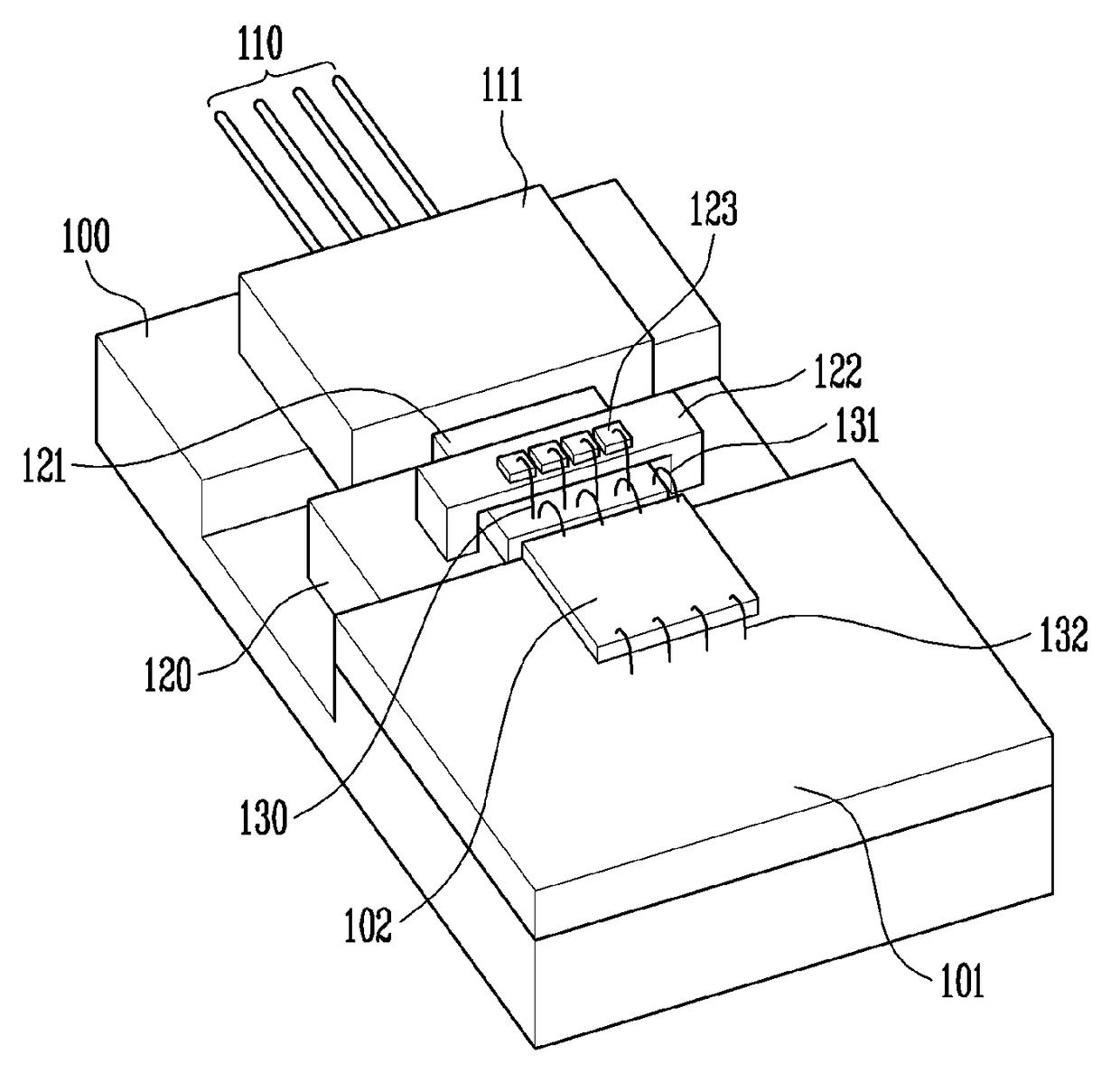
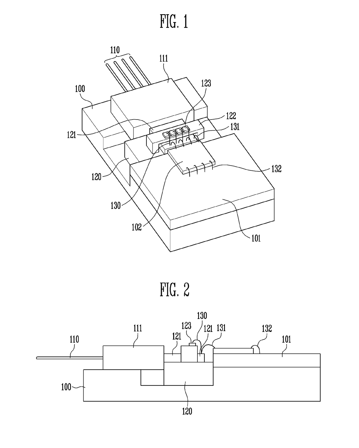
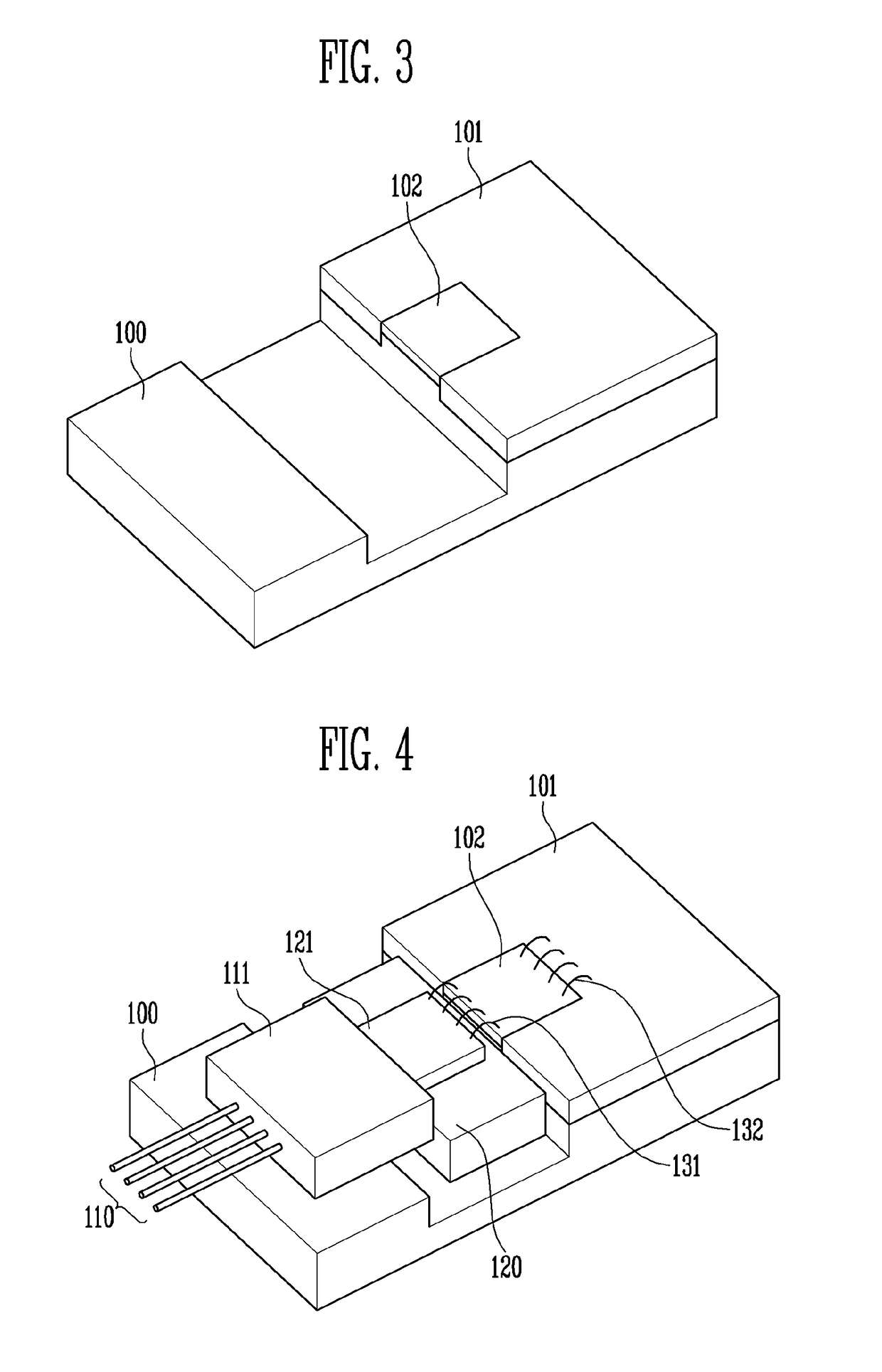
[0038]Hereinafter, embodiments of the present invention will be described in detail with reference to the accompanying drawings.

[0039]In describing the present invention, if an embodiment has been well known in the art to which the present invention pertains and technical contents is not directly related to an embodiment of the present disclosure, descriptions thereof will be omitted. This is to allow the embodiment of the present invention to be clearly understood without obscuring the gist of the embodiment of the present disclosure.

[0040]It is to be understood that when one element is referred to as being “connected to” or “coupled to” another element, it may be connected directly to or coupled directly to another element or be connected to or coupled to another element, having the other element intervening therebetween. In addition, in the following description, and the word ‘including’ does not preclude the presence of other components and means that an additional component is ...


PUM


Abstract

There is provided a receiver optical module including a photodetector having a plurality of channels, a capacitor disposing block formed on an upper portion of the photodetector, a plurality of capacitors formed on the capacitor disposing block, and an electrical wiring configured to connect the plurality of capacitors to electrodes of a plurality of channels of the photodetector, wherein the plurality of capacitors are formed on the capacitor disposing block such that distance between the capacitors and the electrodes of the corresponding channels are the same. Distortion and loss of signal characteristics of high frequency can be reduced and quality of a signal can be enhanced.

Description

CROSS-REFERENCE TO RELATED APPLICATION[0001]This application claims priority to and the benefit of Korean Patent Application No. 10-2015-0066734, filed on May 13, 2015, in the Korean Intellectual Property Office, the entire contents of which are incorporated herein by reference in their entirety.BACKGROUND[0002]1. Field[0003]An embodiment of the present invention relates to a broadcasting communication module, and more particularly, to a receiver optical module structure[0004]2. Description of the Related Art[0005]An optical receiver module (or a receiver optical module) may include an optical signal input unit, a photoelectric conversion unit, a high frequency signal amplifying / processing unit, and a high frequency signal output unit. In particular, an optical receiver module receiving a signal of 10 Gbps or higher should be designed and manufactured in consideration of loss, reflection, and resonance of a high frequency signal with respect to module components and a layout structu...

Claims


Application Information

Patent Timeline
Patent Type & Authority Patents(United States)
IPC IPC(8): H01L31/0232H04B10/25G02B6/00
CPCG02B6/00H04B10/2504G02B6/4249G02B6/4279H04B10/25891
Inventor LEE, SEO YOUNGHAN, YOUNG TAKKIM, JONG HOICHOE, JOONG SEONYOUN, CHUN JUJUNG, HYUN DO
Owner ELECTRONICS & TELECOMM RES INST
Why Eureka
Try Eureka