Method for preparing electrode

a technology of electrodes and substrates, applied in the field of electrode preparation, can solve the problems of low yield of electrodes of array substrates, and achieve the effects of high yield rate, accurate shape control, and precise process control

Active Publication Date: 2018-02-20
TCL CHINA STAR OPTOELECTRONICS TECH CO LTD
View PDF2 Cites 3 Cited by
  • Summary
  • Abstract
  • Description
  • Claims
  • Application Information

AI Technical Summary

Benefits of technology

[0030]The method for preparing electrode of the embodiment of the present disclosure, as a result of the dry etching process forming the receiving area, the etching directional of the dry etching process is strong, and the process control is precise, it is possible to accurately control the shape of the outer contour of the receiving area, that can accurately control the shape of the electrode filled in the receiving area, e.g., the Taper Angle and the CD Loss of the electrodes, so that the yield rate of the electrode is high. Of course, with respect to the wet etching process of the prior art, the dry etching process without using the expensive etching solution (e.g., an acid copper solution), such that the production cost of the electrodes are low.
[0031]At the same time, since the electrode is filled in the receiving area, i.e. the electrode embedded in the buffer layer, so the sides of the electrode can be well protected, to reduce the oxidation risk of the electrode, further improve the yield of the electrode.
[0032]Furthermore, the Taper Angle of the electrode is vertical angle or near vertical angle is not sharp, and therefore can reduce the risk of the occurrence of the electrode tip discharge, to further improve the yield of the electrode.

Problems solved by technology

However, the wet etching process is difficult to accurately adjust the Taper Angle of the electrode and the CD Loss, which led to low yields of the electrode of the array substrate.

Method used


Image

  • Method for preparing electrode
  • Method for preparing electrode
  • Method for preparing electrode

Examples


Embodiment Construction

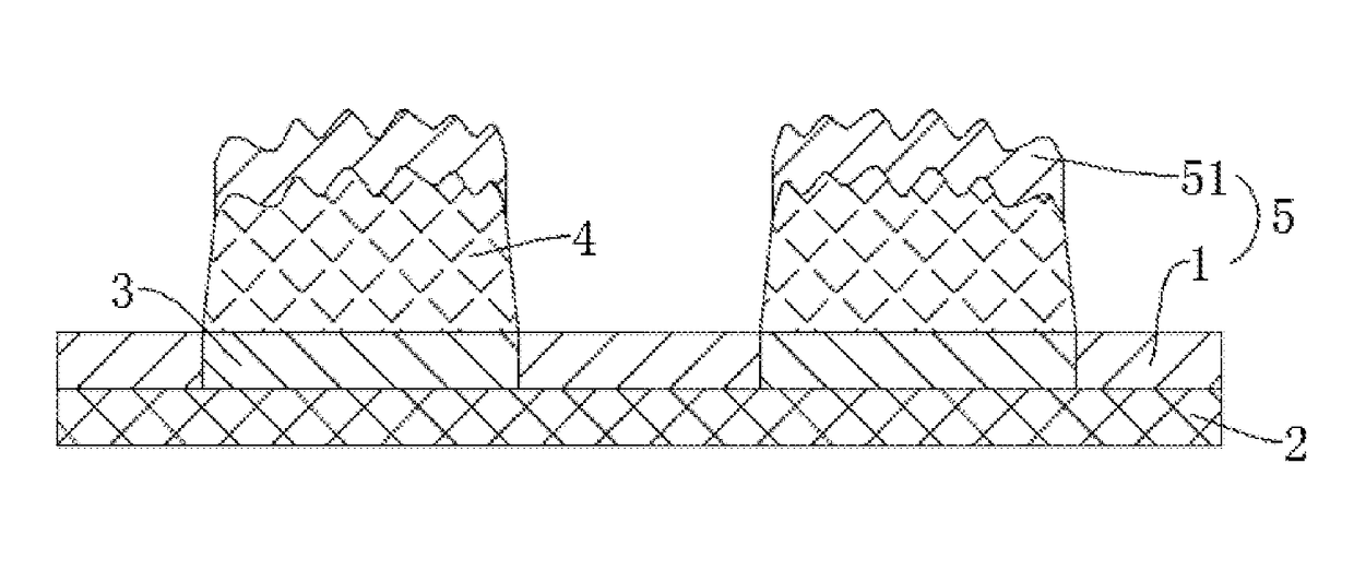
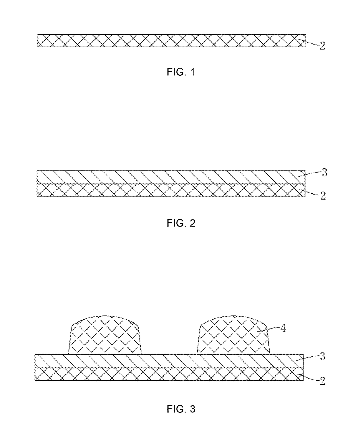
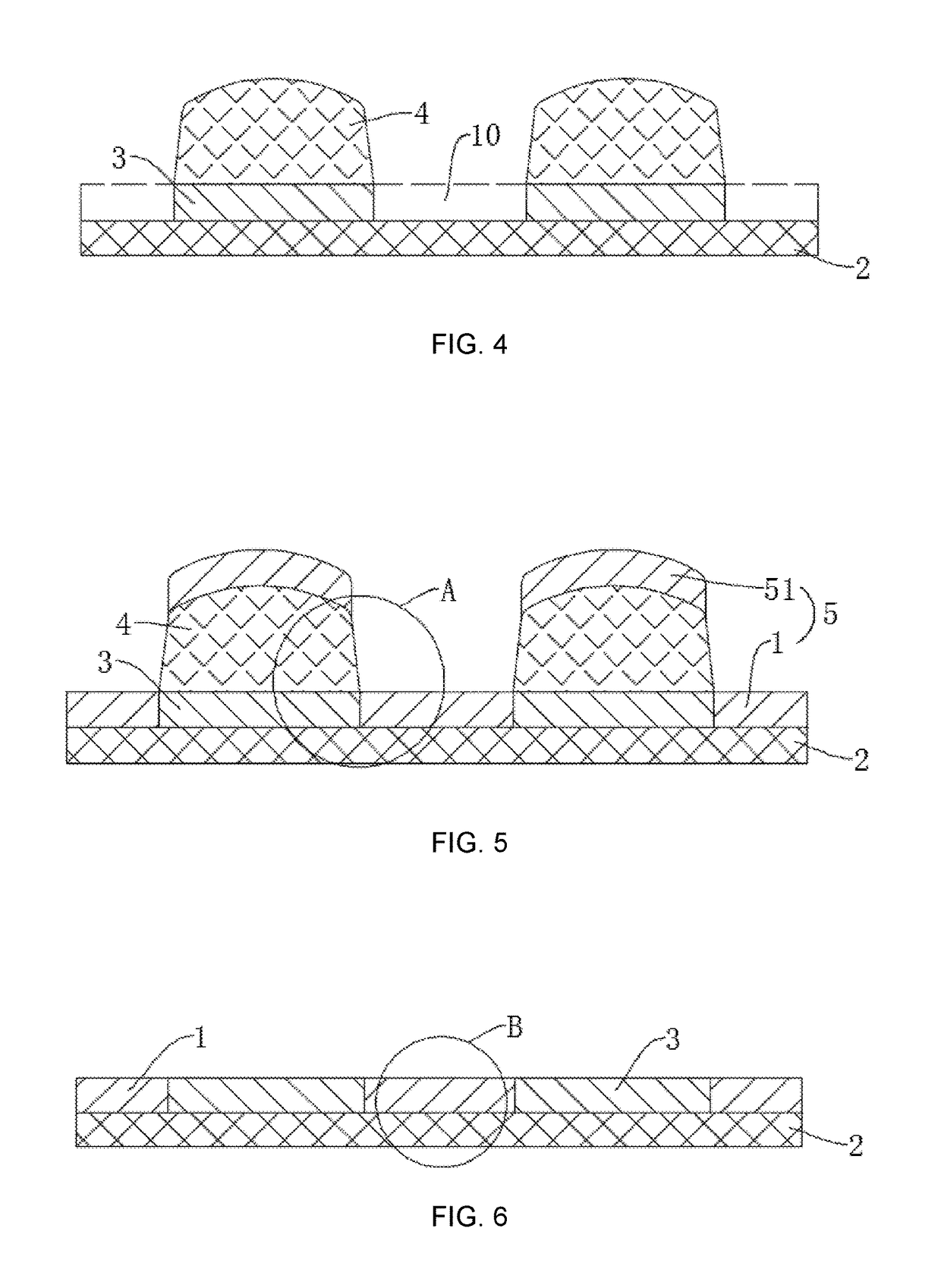
[0039]The present disclosure will now be combined with the implementation of the accompanying drawings, were clear examples of technical solutions of the present disclosure, fully described, it is clear that the described embodiments are merely part of the embodiments of the present disclosure, but not all embodiments Example. Based on the embodiments of the present disclosure, those of ordinary skill in not making all other embodiments without creative efforts obtained, are within the scope of the present disclosure is protected.

[0040]In addition, the following description of embodiments with reference to the attached diagram for illustrating particular embodiments may be used to embodiments of the present disclosure. Term direction of the present disclosure are mentioned, for example, “upper”, “lower”, “front”, “rear”, “left”, “right”, “inside”, “outside”, “side” and so on, only with reference to the accompanying drawings, direction, and thus, the direction of terms used in order ...


PUM

PropertyMeasurementUnit
75°≦α≦90°aaaaaaaaaa
areaaaaaaaaaaa
conductiveaaaaaaaaaa

Abstract

The present disclosure discloses a method for preparing electrode including: providing a substrate; forming a buffer layer on the substrate; forming a patterned photoresist on the surface of the buffer layer away from the substrate, the photoresist has a bottom surface and a top surface disposed opposite and a side connected between the bottom surface and the top surface, the bottom surface is bonded to the buffer layer; by dry etching, the portions of the photoresist not covered by the buffer layer is removed to form a receiving area; depositing a conductive film, the conductive film layer includes a waste material forming on the top surface and an electrode filling in the receiving area; and stripping the waste material and the photoresist. The yields of the method for preparing electrode of the present disclosure is high.

Description

CROSS REFERENCE[0001]The present disclosure claims the priority of No. 201610436577.6, entitled “method for preparing electrode”, filed on Jun. 17, 2016, the disclosure of which is incorporated herein by reference in its entirety.FIELD OF THE DISCLOSURE[0002]The present disclosure relates to an array substrate preparing technology field, and more particularly to a method for preparing an electrode.BACKGROUND OF THE DISCLOSURE[0003]In the liquid crystal display panel industry, the current electrode in the array substrate of the LCD panel is generally used the wet etching process to patterned. However, the wet etching process is difficult to accurately adjust the Taper Angle of the electrode and the CD Loss, which led to low yields of the electrode of the array substrate.SUMMARY OF THE DISCLOSURE[0004]The technical problem to be solved by the present disclosure is to provide a method for preparing a high yield electrode can be used to prepare the electrode of the array substrate.[0005...

Claims


Application Information

Patent Timeline
Patent Type & Authority Patents(United States)
IPC IPC(8): H01L21/44H01L21/04H01L21/28H01L21/82
CPCH01L21/0425H01L21/82H01L21/28123H01L27/1259G02F1/13439H01L29/78603H01L27/1218H01L27/124H01L27/1288
Inventor ZHOU, ZHICHAOXIA, HUI
Owner TCL CHINA STAR OPTOELECTRONICS TECH CO LTD
Why Eureka
Try Eureka