Tunable nano-antenna and methods of manufacturing and operating the same

a nano-antenna and nano-particle technology, applied in the field of nano-antennas, can solve the problems of ineffective optical nano-antennas of the related art to function as transmitters and receivers in various wavelengths, and achieve the effect of wide optical bandwidth and increased utilization of optical nano-antennas of the present disclosur

Active Publication Date: 2018-02-27
SAMSUNG ELECTRONICS CO LTD
View PDF23 Cites 8 Cited by
  • Summary
  • Abstract
  • Description
  • Claims
  • Application Information

AI Technical Summary

Benefits of technology

[0023]The tunable optical nano-antenna of the present disclosure includes a wavelength-tunable material layer. The tenability of the wavelength-tunable material layer may be controlled in an electric, optical, or thermal manner depending on a tunable material layer. Thus, the optical nano-antenna may be utilized as an optical nano-antenna having a wide optical bandwidth, or may be utilized as an active element that may be controlled in real time by various control methods. Therefore, the utilization of the optical nano-antenna of the present disclosure may increase as compared with a passive optical nano-antenna of the related art.

Problems solved by technology

However, there is a limitation that the antennas formed of nanoparticles can transmit and receive only light having a single wavelength.
Thus, optical nano-antennas of the related art are not so effective to function as transmitters-receivers in various wavelengths.

Method used


Image

  • Tunable nano-antenna and methods of manufacturing and operating the same
  • Tunable nano-antenna and methods of manufacturing and operating the same
  • Tunable nano-antenna and methods of manufacturing and operating the same

Examples


Embodiment Construction

Technical Problem

[0003]Provided are active-type optical nano-antennas, which are wavelength-tunable antennas and capable of switching.

[0004]Provided are methods of manufacturing the tunable optical nano-antennas.

[0005]Provided are methods of operating the tunable optical nano-antennas.

Technical Solution

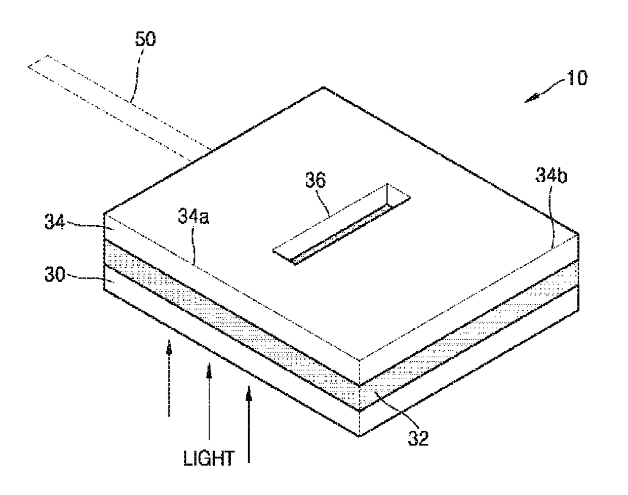
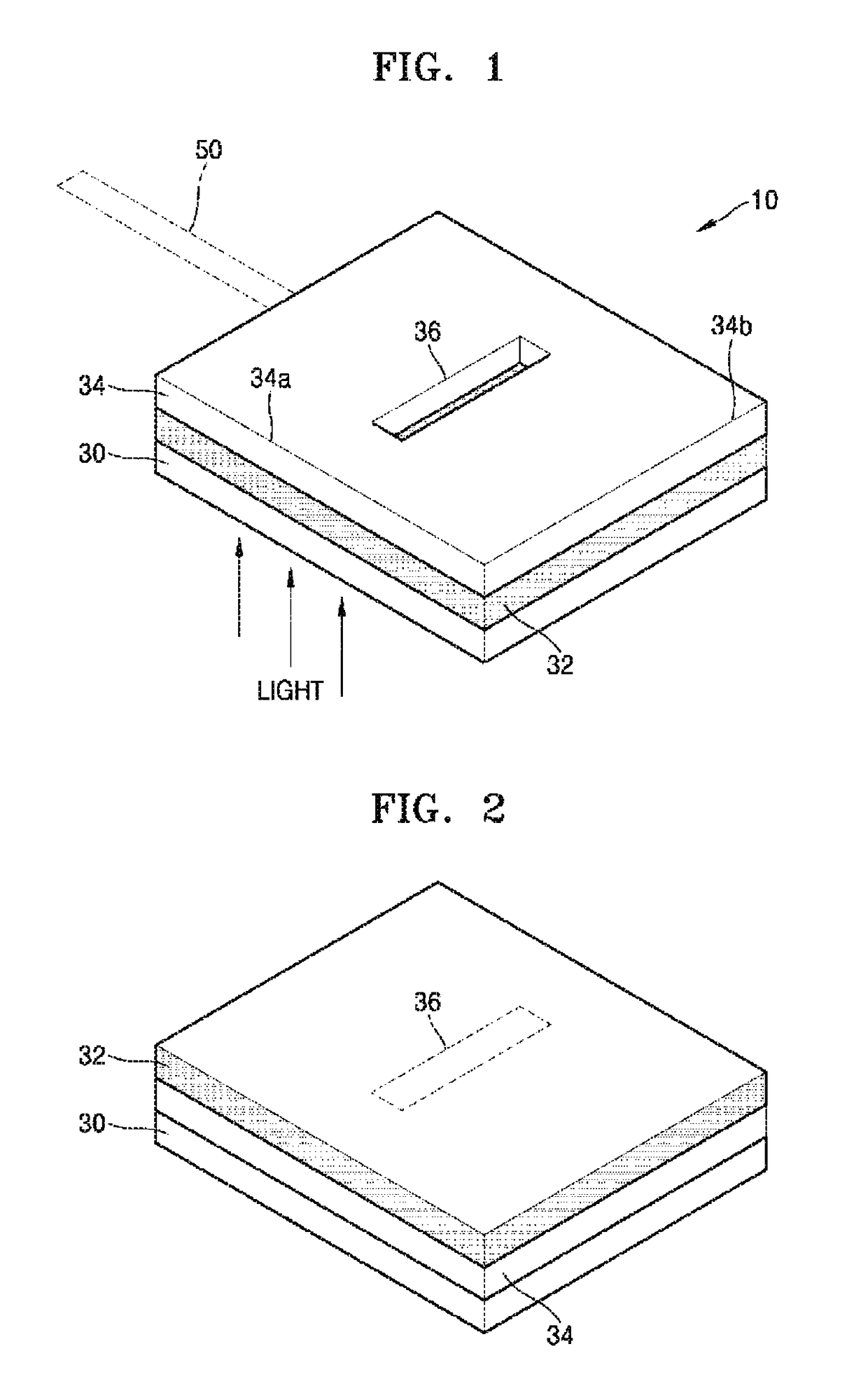
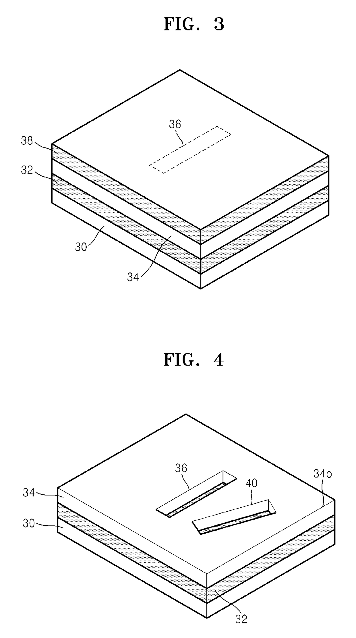
[0006]According to an aspect of the present invention, an optical nano-antenna includes: a substrate; and a plurality of material layers sequentially laminated on the substrate; wherein the plurality of material layers include at least one tunable material layer and at least one slot.

[0007]A first tunable material layer and a metal layer may be sequentially laminated on the substrate, and a first slot may be formed in the metal layer.

[0008]A metal layer and a first tunable material layer may be sequentially laminated on the substrate, and a first slot may be formed in the metal layer.

[0009]A first tunable material layer, a metal layer, and a second tunable material layer may be sequen...


PUM

PropertyMeasurementUnit
wavelengthaaaaaaaaaa
thicknessaaaaaaaaaa
optical characteristicaaaaaaaaaa

Abstract

Provided are an optical nano-antenna including a tunable material layer and methods of manufacturing and operating the optical nano-antenna. The optical nano-antenna includes a substrate; and a plurality of material layers sequentially laminated on the substrate. The plurality of material layers include at least one tunable material layer and at least one slot. A first tunable material layer and a metal layer are sequentially laminated on the substrate, and a first slot is formed in the metal layer. A metal layer and a first tunable material layer are sequentially laminated on the substrate, and a first slot is formed in the metal layer. A first tunable material layer, a metal layer, and a second tunable material layer are sequentially laminated on the substrate, and a first slot is formed in the metal layer. A second slot tilted with respect to the first slot is formed in the metal layer.

Description

TECHNICAL FIELD[0001]The present disclosure relates to antennas, and more particularly, to wavelength-tunable optical nano-antennas and methods of manufacturing and operating the same.BACKGROUND ART[0002]Optical nano-antennas are kinds of optical devices that receive light and convert the received light into an electromagnetic field or perform an opposite function thereto. Radio waves used for mobile phone communication have a wavelength of approximately several cm. Thus, antennas for mobile phone communication have a certain degree of size. However, a wavelength of light is as extremely low as approximately 500 nm. For this reason, optical nano-antennas have to be made as thin as approximately 100 nm, which is a hundred-thousandth the thickness of human hair. It is possible to manufacture such minute antennas in accordance with the development of nanotechnology. However, there is a limitation that the antennas formed of nanoparticles can transmit and receive only light having a sin...

Claims


Application Information

Patent Timeline
Patent Type & Authority Patents(United States)
IPC IPC(8): B82Y20/00B82Y40/00H01Q5/22G02B6/12G02F1/01H01Q13/18H01Q13/10H01Q13/28G02F1/00
CPCG02F1/0102B82Y20/00B82Y40/00G02B6/12007G02F1/011H01Q13/103H01Q13/18H01Q13/28H01Q5/22G02F1/0045G02B2006/12142G02F1/0018G02B6/1226G02F2/02H01Q1/24H01Q13/10
Inventor PARK, YEONSANGKIM, JINEUNROH, YOUNGGEUNLEE, CHANGWONCHEON, SANGMOKIM, UNJEONGBAIK, CHANWOOKYOON, YOUNGZOONLEE, JAESOONG
Owner SAMSUNG ELECTRONICS CO LTD
Why Eureka
Try Eureka