
Liquid crystal panel and fabricating method thereof

a technology of liquid crystal panels and fabrication methods, applied in non-linear optics, instruments, optics, etc., can solve the problems of high fabricating cost and complex fabricating art required to form pss with different heights, and achieve the effect of saving cost and simplifying fabricating ar

Active Publication Date: 2018-04-03
WUHAN CHINA STAR OPTOELECTRONICS TECH CO LTD
View PDF12 Cites 0 Cited by
  • Summary
  • Abstract
  • Description
  • Claims
  • Application Information

AI Technical Summary

Benefits of technology

The present invention is a new method for making liquid crystal panels that simplifies the process and reduces the cost. This is achieved by making different colored resists on the color film substrate and creating spacers with the same height on the array substrate. This allows for the creation of the first and second spacers in one step, reducing the number of steps and making the fabrication process more efficient. This new method also maintains the thickness of the liquid crystal panel, ensuring clear display of images.

Problems solved by technology

Therefore, when the liquid crystal panel is made by the present technique, a complex fabricating art is required to form the PSs with different heights.
In addition, using an expansive mask results a high fabricating cost, too.

Method used


Image

  • Liquid crystal panel and fabricating method thereof
  • Liquid crystal panel and fabricating method thereof
  • Liquid crystal panel and fabricating method thereof

Examples


first embodiment

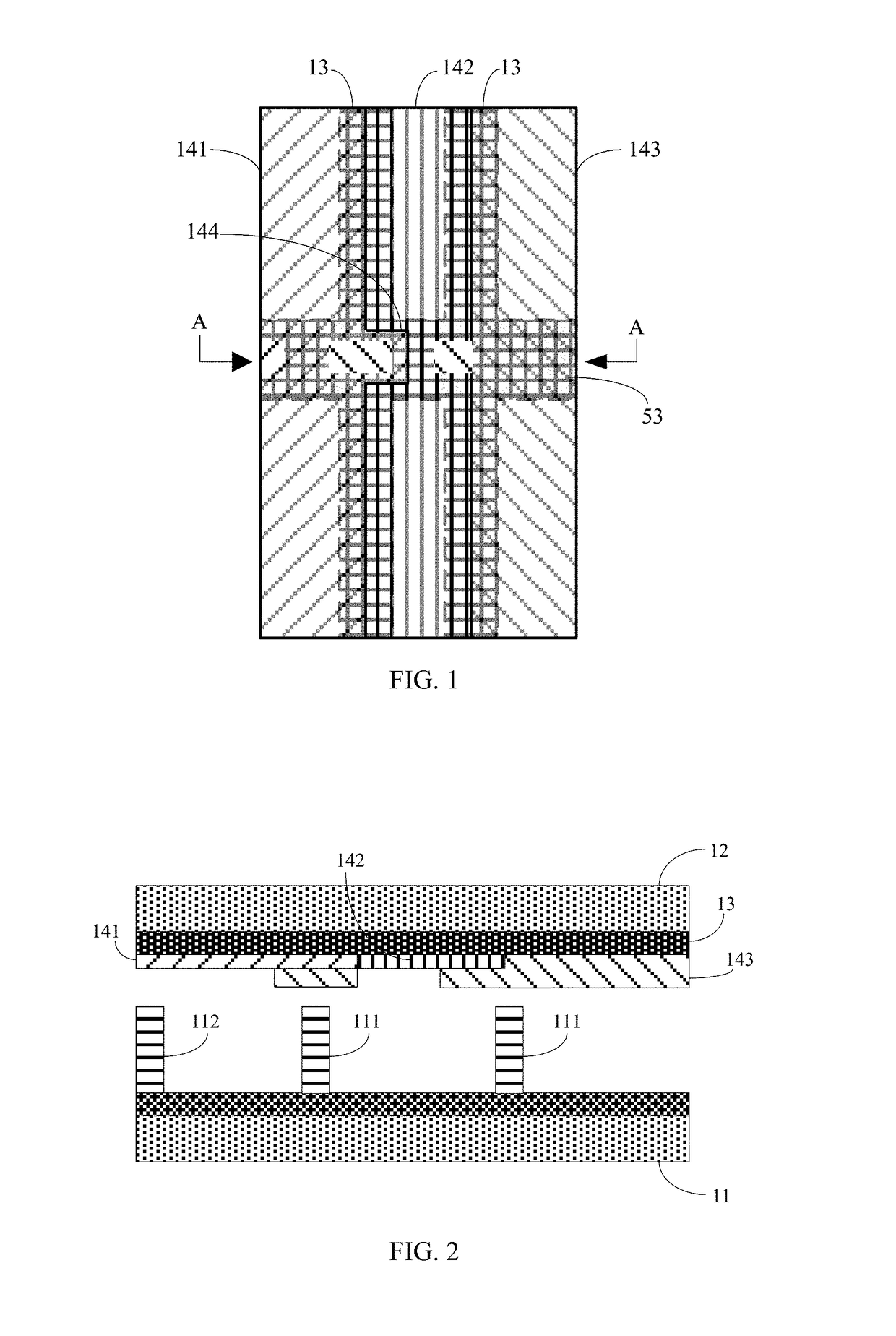
[0033]With reference to FIG. 1 and FIG. 2, FIG. 1 is a structural schematic view of a color film substrate of a liquid crystal of the present invention. FIG. 2 is a cross sectional schematic view taken along A-A line of FIG. 1.

[0034]The liquid crystal panel of the present invention has an array substrate 11, a color film substrate 12 and a liquid crystal layer (not shown in the drawing) mounted between the array substrate 11 and the color film substrate 12.

[0035]The color film substrate 12 has multiple color resists formed thereon and the color resists are formed to multiple color filter units. Particularly, the liquid crystal panel of the present embodiment is an RGB display mode. The color resists of the color film substrate 12 includes a red color resist 141, a green color resist 142 and a blue color resist 143. The red color resist 141 is formed to a red filter unit, the green color resist 142 is formed to a green filter unit and the blue color resist 143 is formed to a blue fil...

second embodiment

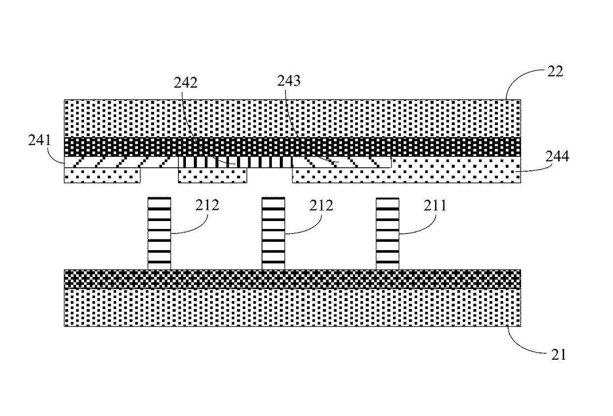
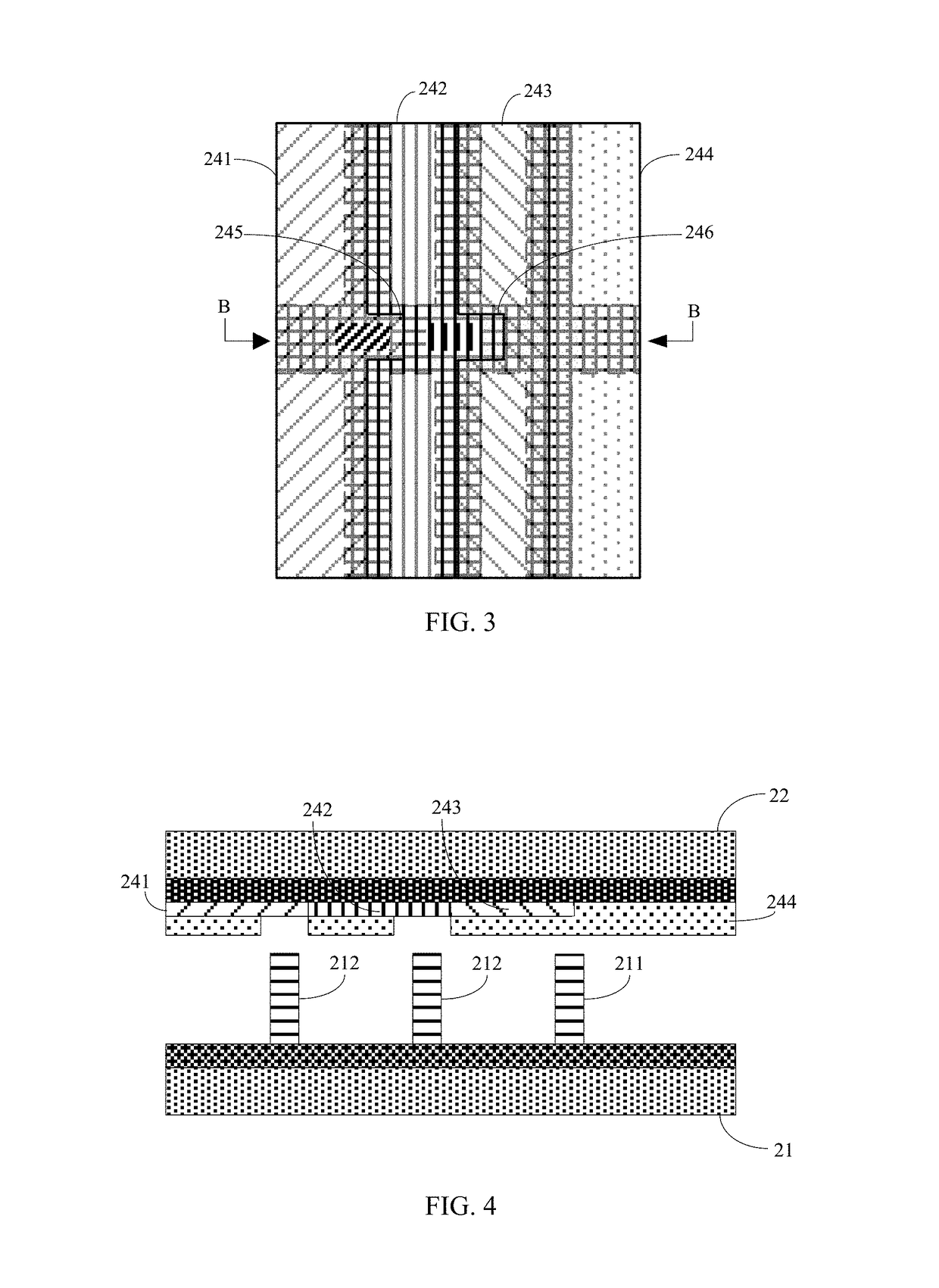
[0050]With reference to FIG. 3 and FIG. 4, FIG. 3 is structural schematic view of the color film substrate of the liquid crystal panel of the present invention. FIG. 4 is a cross sectional schematic view taken along B-B line of FIG. 3.

[0051]A difference between the present embodiment and the first embodiment is that the liquid crystal panel of the present embodiment is an RGBW display module. The color film substrate 22 has four different color resists formed thereon and including the red color resist 241, the green color resist 242, the blue color resist 243 and the white color resist 244. The red, green and blue color resists 241, 242, 243 have the same thickness and the white color resist 244 is thicker than the red color resist 241. For example, the white color resist 244 is 0.3 μm or 0.5 μm thicker than the red color resist 241. It should be noted that the white color resist 244 of the present invention may be used as a flat layer to provide the color film substrate 22 a flat f...

third embodiment

[0059]With reference to FIG. 5 and FIG. 6, FIG. 5 is a structural schematic view of the color film substrate of the liquid crystal panel of the present invention. FIG. 6 is a cross sectional schematic view taken along C-C line of FIG. 5.

[0060]The liquid crystal panel of the present embodiment is an RGB display mode, the color film substrate 32 of the liquid crystal panel has the red, green and blue color resists 341, 342, 343 formed thereon. The red and green color resists 341, 342 have the same thickness, and the blue color resist 343 is thicker than the red color resist 341.

[0061]The array substrate 31 has the first, second and third spacers 311, 312, 313 formed thereon. Further, the first and second spacers 311 and 312 have the same height. The blue color resist 343 corresponding to the first spacer 311 is thicker than the red color resist 341 corresponding to the second spacer 312.

[0062]The third spacer 313 is higher than the second spacer 312. The color resist corresponding to ...


PUM

PropertyMeasurementUnit
thicknessesaaaaaaaaaa
thicknessaaaaaaaaaa
thicknessaaaaaaaaaa

Abstract

The present disclosure provides a liquid crystal panel and a fabricating method thereof. The liquid crystal panel has an array substrate, a color film substrate and a liquid crystal layer mounted between the array substrate and the color film substrate. The color film substrate forms multiple color resists thereon to form multiple color filter units. The array substrate at least forms a first spacer and a second spacer thereon. A height of the first spacer is equal to a height of the second spacer. A thickness of the color resist corresponding to the first spacer is different from a thickness of the color resist corresponding to the second spacer. The present disclosure simplifies a fabricating art, saves cost and effectively maintains a thickness of the liquid crystal panel at the time to ensure that the liquid crystal panel can clearly display image.

Description

FIELD OF THE INVENTION[0001]The present invention relates to liquid crystal display field, especially to a liquid crystal panel and a fabricating method thereof.BACKGROUND OF THE INVENTION[0002]As a development of liquid crystal display tending to high pixels per inch (PPI), a technique of low temperature poly-silicon (LTPS) gradually replaces a technique of amorphous silicon.[0003]The LTPS TFT array substrate generally employs an over coating flat layer, so the LTPS TFT array substrate does not like that the technique of amorphous silicon (without over coating) uses height differences among layers of an array substrate to form multiple photo spacers (PS) having the same height on a side of a color film substrate (CF) to form main PS and sub-PS structures. Therefore, LTPS usually needs a halftone technique to form the PSs with two different heights on the side of the CF to be used as the main PS and the sub-PS. If three PSs with different heights are required, a gray tone technique ...

Claims


Application Information

Patent Timeline
Patent Type & Authority Patents(United States)
IPC IPC(8): G02F1/1339G02F1/1335
CPCG02F1/133514G02F1/13394G02F1/133516G02F1/133512G02F2001/13396G02F1/1333G02F1/1339G02F1/13396
Inventor TANG, YUEJUN
Owner WUHAN CHINA STAR OPTOELECTRONICS TECH CO LTD
Learn More