Imaging system

a technology of imaging system and image, applied in the field of imaging system, can solve the problems of difficult miniaturization of the system, huge technical challenge, and use of lenses, mirrors or beam splitters, and achieve the effect of improving the image system, improving the image contrast, and improving the performance of the image system

Inactive Publication Date: 2018-04-10
CSEM CENT SUISSE DELECTRONIQUE & DE MICROTECHNIQUE SA RECH & DEV
View PDF24 Cites 22 Cited by
  • Summary
  • Abstract
  • Description
  • Claims
  • Application Information

AI Technical Summary

Benefits of technology

[0010]Compared to imaging devices of prior art the imaging system of the invention does not need optical elements to be aligned and assembled at the illumination distal end. The main advantage of the imaging system compared to systems of prior art is that the illuminating and light collecting portion of the waveguide may be introduced in very narrow places, or places that have a difficult access, such as curved pipes. Also, because of the simplicity of the design the imaging system may be very cheap. A part of the critical improvement is due to the very low aspect ratio of diffraction gratings. Surface diffraction gratings are typically thinner than one micron and allow to redirect a light beam efficiently without needed to be substantially perpendicular to the light propagation axis before or after redirection. The diffracted angle is not dependent only of the grating orientation compared to the incidence angle of the light beam but of the grating period. This allows vast design flexibility and extremely flat aspect ratio structures to redirect light beams.
[0035]Said first diffraction grating and / or said second diffractive grating and / or third diffractive grating may comprise, each, a series of diffraction gratings, said gratings may be arranged to provide a plurality of outcoupled and / or incoupled light beams, said plurality of outcoupled and / or incoupled light beams being not parallel. Providing a plurality of non-parallel light beams to illuminate an object and recollect the returned light by the reflection of a portion of said non parallel beams allows to provide an image system that may perform a distance analysis of the object and / or to perform a 3D analysis of at least a part of the surface of said object, by using well known optical parallax effects. Said first diffraction grating and / or said second diffractive grating and / or third diffractive grating may comprise a non-homogenous grating or an hologram, allowing to create one or a plurality of non parallel light beams, such as but not limited to converging or diverging light beams, using wavefront shaping diffractive optical elements.

Problems solved by technology

This has been necessitated by the need to access hostile, space-limited or difficult environments.
The use of lenses, mirrors or beam-splitters is a fundamental limitation on the size reduction of this kind of optical inspection systems.
The miniaturization of concepts using these components is a huge technical challenge, especially when side views of the object need to be obtained.
The device disclosed in US2013 / 0317295 is limited in that it would be extremely difficult to miniaturize the system so that the overall cross section of the device is smaller than 3-5 mm.
Again, a basic limitation of the design is the possible miniaturization of the device because of the use of macroscopic lenses.
Again here most systems rely on the use of lenses and mirrors and the systems are limited to centimeter sized periscopes having centimeter sized cross sections and it is difficult to make periscopes flexible.
Therefore most optical inspection systems based on classical endoscopes, borescopes and periscopes have a limited use where the insertion volumes are extremely small and they are expensive and not realizable in a batch process.
Although the use of MEMS components allows to make innovative devices such as scanning micro endoscopes, the systems are still limited in site as connections have to be made to fiber optics and GRIN or other types of small lenses are required.
Because of the component and assembly costs such systems still have a relative high cost.

Method used


Image

  • Imaging system
  • Imaging system
  • Imaging system

Examples


Embodiment Construction

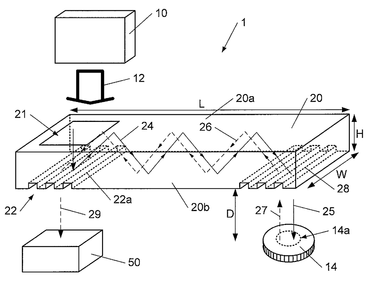
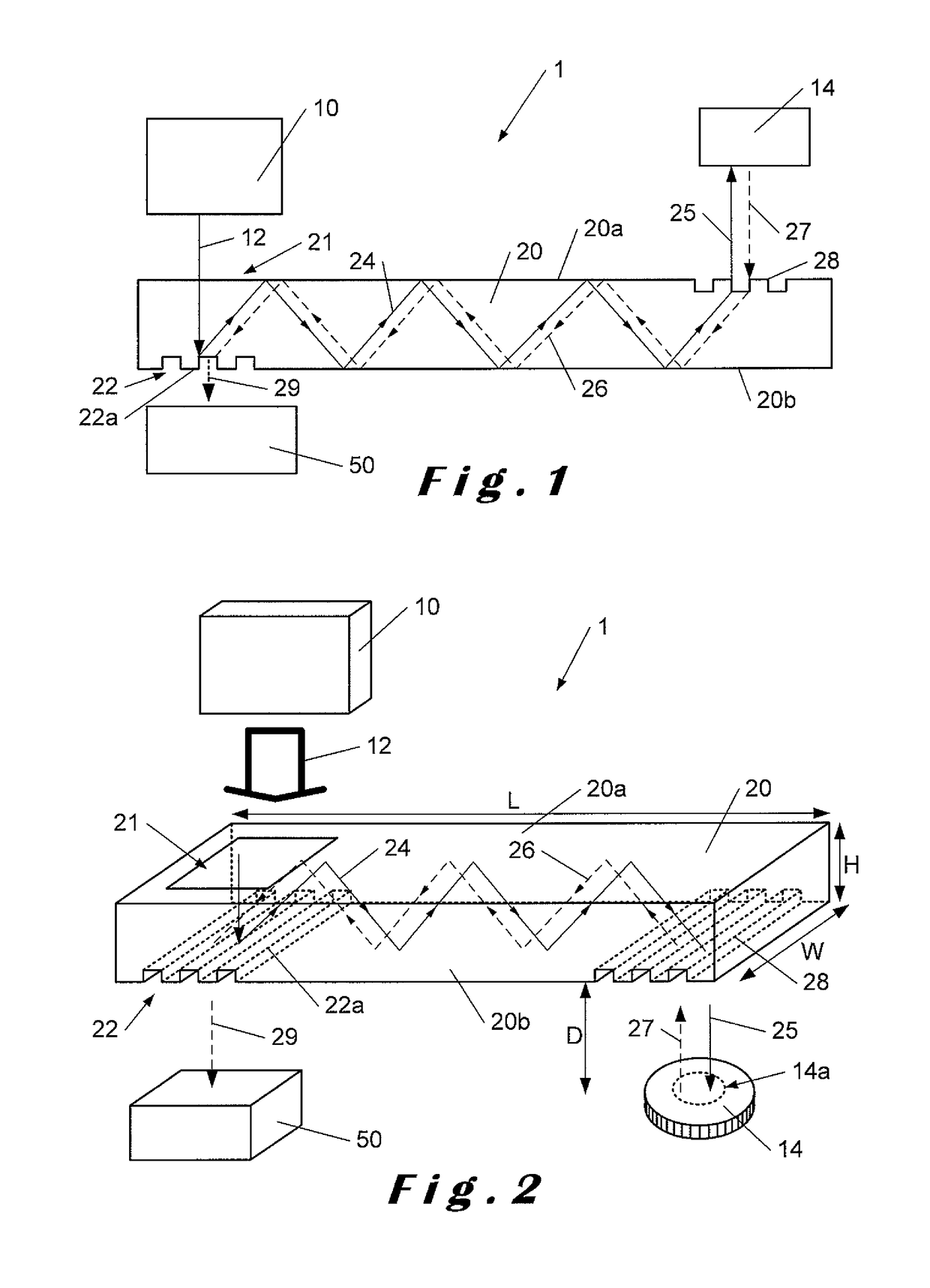
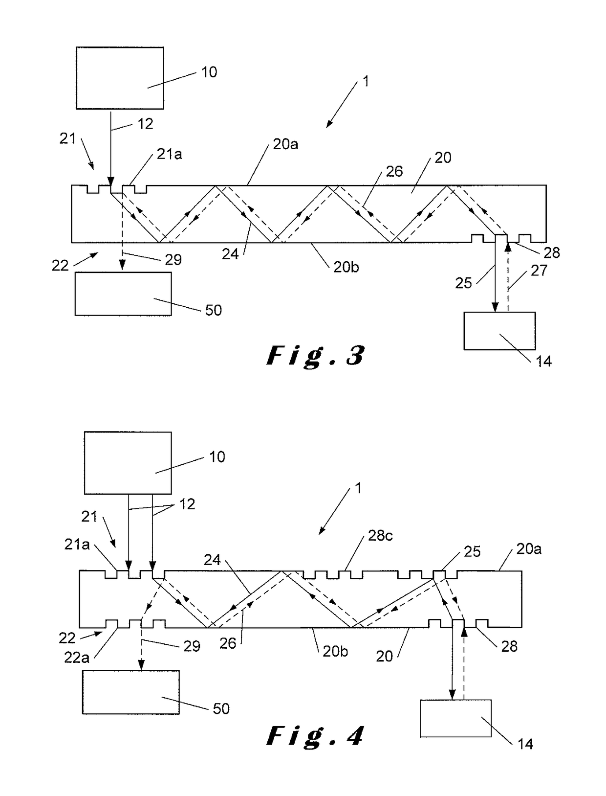
[0043]The following detailed description illustrates the principles and examples of embodiments according to the invention. It will thus be appreciated that those skilled in the art will be able to devise various arrangements that, although not explicitly described or shown herein, embody the outlined principles of the invention and are included in its scope as defined in the claims. In the description and the figures, similar reference signs refer to the same or similar components or structural elements.

[0044]Imaging system 1 according to the invention comprises a light source 10 which is coupled into an optical waveguide 20. A part of the guided light 24 illuminates an object 14 and returned light beam 26 returned by the optical waveguide 20 is directed on an imaging system 50. The imaging system 1 of the invention does not require any optical elements that must be assembled at the extremity of the optical waveguide 20, which simplifies considerably the optical system, makes it mo...


PUM


Abstract

An imaging system suitable to provide an image of a surface portion of an object is disclosed. The system includes a light source arranged to provide a light beam, at least a first optical waveguide having a first face and having a second face opposite to the first face, the first face having an incoupling surface. The optical waveguide includes an outcoupling surface, a first diffraction grating arranged on the optical waveguide, and an imaging subsystem arranged to the outcoupling surface. The first diffraction grating is arranged to outcouple at least a fraction of the light beam.

Description

TECHNICAL FIELD[0001]The present invention relates to imaging systems suitable for inspecting objects or surface portions of an object in equipment having very little space to insert the distal ends of said optical systems. More specifically the present invention relates to an imaging system based on a slim optical device using an optical waveguide, to guide an illumination beam and to form, by the returned light beam, an image.BACKGROUND OF THE INVENTION[0002]There has been an immense drive in modern optical inspection systems towards miniaturization. This has been necessitated by the need to access hostile, space-limited or difficult environments. Typical fields in which extreme miniaturization of optical inspections systems are developed are: medical endoscopes, borescopes for the inspection of tubes with small diameters, industrial machinery, a wide variety of systems such as security systems based on optical readout. Also, along with the development and widely available microsy...

Claims


Application Information

Patent Timeline
Patent Type & Authority Patents(United States)
IPC IPC(8): G02B23/24F21V8/00
CPCG02B23/2461G02B23/2423G02B6/0036G02B6/0016G02B6/00G02B23/26
Inventor BASSET, GUILLAUMEGALLINET, BENJAMINSATILMIS, BRUNO
Owner CSEM CENT SUISSE DELECTRONIQUE & DE MICROTECHNIQUE SA RECH & DEV
Why Eureka
Try Eureka