Integrated circuit packages including high density bump-less build up layers and a lesser density core or coreless substrate

a technology of integrated circuits and build-up layers, applied in the direction of electrical equipment, semiconductor devices, semiconductor/solid-state device details, etc., can solve the problems of reducing pitch and increasing complexity of traditional flip-chip processes

Active Publication Date: 2018-04-10
INTEL CORP
View PDF119 Cites 149 Cited by
  • Summary
  • Abstract
  • Description
  • Claims
  • Application Information

AI Technical Summary

Problems solved by technology

Traditional flip chip processes become increasingly complex as bump pitch reduces because of the difficulty in under filling the space between the flip chip bumps.

Method used


Image

  • Integrated circuit packages including high density bump-less build up layers and a lesser density core or coreless substrate
  • Integrated circuit packages including high density bump-less build up layers and a lesser density core or coreless substrate
  • Integrated circuit packages including high density bump-less build up layers and a lesser density core or coreless substrate

Examples


Embodiment Construction

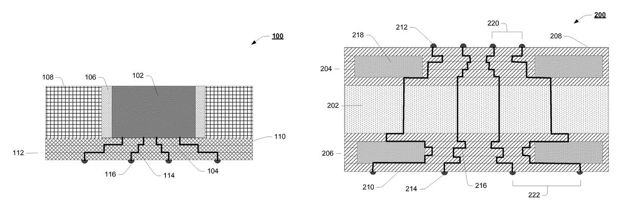
[0008]In the following description, for purposes of explanation, numerous specific details are set forth in order to provide a thorough understanding of the invention. It will be apparent, however, to one skilled in the art that embodiments of the invention can be practiced without these specific details. In other instances, structures and devices are shown in block diagram form in order to avoid obscuring the invention.

[0009]Reference throughout this specification to “one embodiment” or “an embodiment” means that a particular feature, structure or characteristic described in connection with the embodiment is included in at least one embodiment of the present invention. Thus, appearances of the phrases “in one embodiment” or “in an embodiment” in various places throughout this specification are not necessarily all referring to the same embodiment. Furthermore, the particular features, structures or characteristics may be combined in any suitable manner in one or more embodiments.

[00...


PUM


Abstract

In some embodiments, integrated circuit packages including high density bump-less build up layers and a lesser density core or coreless substrate are presented. In this regard, an apparatus is introduced having a first element including a microelectronic die having an active surface and at least one side, an encapsulation material adjacent said at least one microelectronic die side, wherein said encapsulation material includes at least one surface substantially planar to said microelectronic die active surface, a first dielectric material layer disposed on at least a portion of said microelectronic die active surface and said encapsulation material surface, a plurality of build-up layers disposed on said first dielectric material layer, and a plurality of conductive traces disposed on said first dielectric material layer and said build-up layers and in electrical contact with said microelectronic die active surface; and a second element coupled to the first element, the second element including a substrate having a plurality of dielectric material layers and conductive traces to conductively couple conductive contacts on a top surface with conductive contacts on a bottom surface, said conductive contacts on said top surface conductively coupled with said conductive traces of said first element. Other embodiments are also disclosed and claimed.

Description

FIELD OF THE INVENTION[0001]Embodiments of the present invention generally relate to the field of integrated circuit package design and, more particularly, to integrated circuit packages including high density bump-less build up layers and a lesser density core or coreless substrate.BACKGROUND OF THE INVENTION[0002]With shrinking transistor size and more functionality incorporated into microelectronic devices, die to package substrate interconnect geometries will also need to be reduced. Currently, the die is connected to the package substrate using a solder joint connection commonly referred to as a flip-chip connection. Traditional flip chip processes become increasingly complex as bump pitch reduces because of the difficulty in under filling the space between the flip chip bumps.BRIEF DESCRIPTION OF THE DRAWINGS[0003]The present invention is illustrated by way of example and not limitation in the figures of the accompanying drawings in which like references indicate similar eleme...

Claims


Application Information

Patent Timeline
Patent Type & Authority Patents(United States)
IPC IPC(8): H01L25/065H01L25/10H01L23/538H01L25/16H01L23/498H01L23/00H01L21/56H01L23/31
CPCH01L25/0652H01L23/5389H01L25/105H01L25/16H01L2924/19043H01L21/563H01L23/3128H01L23/49827H01L24/13H01L24/16H01L2224/05548H01L2224/05573H01L2225/1023H01L2225/1058H01L2924/00014H01L2924/14H01L2924/1433H01L2924/15174H01L2924/15311H01L2924/18161H01L2924/19041H01L2924/19042H01L2224/05599H01L2224/02379
Inventor SKEETE, OSWALDMAHAJAN, RAVIGUZEK, JOHN
Owner INTEL CORP
Why Eureka
Try Eureka