Semiconductor packing structure and production thereof

A packaging method and semiconductor technology, applied in the fields of semiconductor/solid-state device manufacturing, semiconductor devices, semiconductor/solid-state device components, etc., to achieve the effect of increasing production capacity, saving consumption, and reducing glue spillage

Active Publication Date: 2007-12-19
ADVANCED SEMICON ENG INC
View PDF3 Cites 1 Cited by
  • Summary
  • Abstract
  • Description
  • Claims
  • Application Information

AI Technical Summary

Problems solved by technology

[0006] The main purpose of the present invention is to overcome the defects existing in the existing semiconductor packaging structure and provide a new semiconductor packaging structure. The technical problem to be solved

Method used


Image

  • Semiconductor packing structure and production thereof
  • Semiconductor packing structure and production thereof
  • Semiconductor packing structure and production thereof

Examples


Example Embodiment

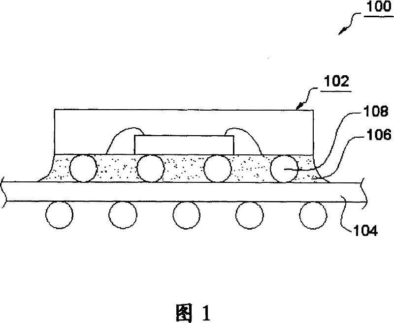
[0055] In order to further explain the technical means and effects that the present invention adopts to achieve the intended purpose of the invention, the specific structure, manufacturing method, and steps of the semiconductor package structure and its manufacturing method proposed according to the present invention will be described below in conjunction with the accompanying drawings and preferred embodiments. , features and their effects are described in detail below.

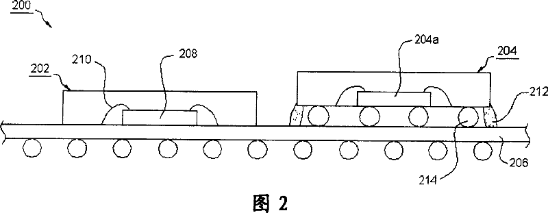
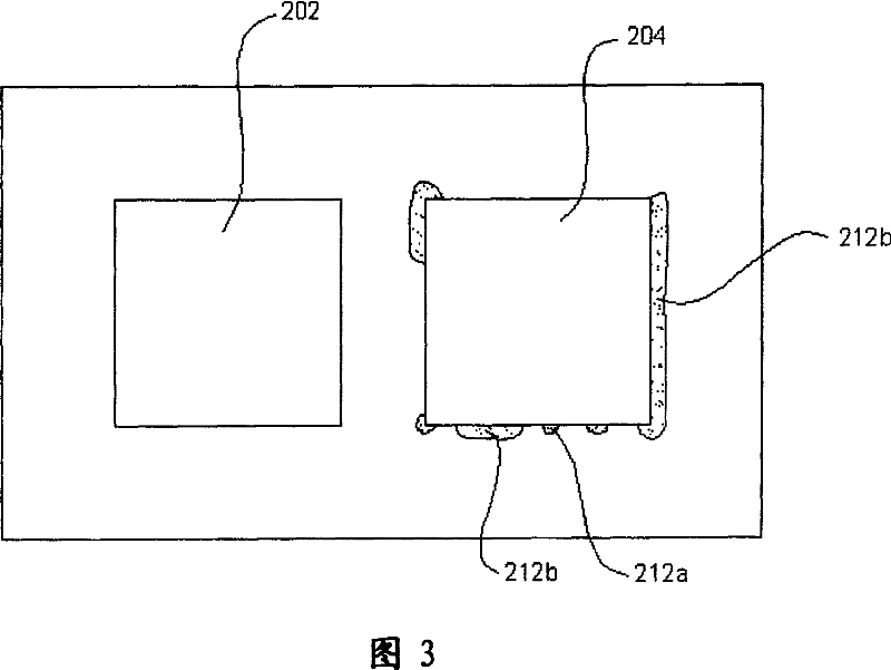
[0056] Please refer to FIG. 2 , which is a cross-sectional view of a semiconductor package structure according to an embodiment of the present invention. A semiconductor package structure 200 according to an embodiment of the present invention mainly includes a first semiconductor device 202 and a second semiconductor device 204 , wherein both the first semiconductor device 202 and the second semiconductor device 204 are a semiconductor package structure. The first semiconductor device 202 includes a substra...


PUM


Abstract

The construction of semiconductor encapsulation mainly consists of a baseboard and a semiconductor component connected with base board by using Flip Chip Bonding. A link construction is set between the semiconductor and base board, and extends along with underside of the semiconductor component in order to press the semiconductor component on the base board. The link construction is formed by solidifying sticking agent, and has function of fixing connection and supporting. The method of semiconductor encapsulation is: a semiconductor component is set on base board and is connected with base board by using Flip Chip bonding; the sticking agent is coated along with underside of semiconductor encapsulation; at least one sticking construction is formed between the edge of underside of semiconductor component and base board, and is used to fix the semiconductor component on the base board.

Description

technical field [0001] The invention relates to a semiconductor packaging structure and a manufacturing method thereof. Background technique [0002] Please refer to FIG. 1 , which is a cross-sectional view of a conventional semiconductor package structure. The conventional semiconductor package structure 100 includes a semiconductor device 102 fixed on a substrate 104 in a flip-chip connection (for example, by a plurality of solder balls 108 ). There is an underfill 106 between the semiconductor element 102 and the substrate 104, thereby increasing the mechanical strength of the joint between the semiconductor element 102 and the substrate 104, and fixing the relative position between the two, so when the semiconductor The packaging structure 100 will not be disintegrated or deformed when it is subjected to high temperature during, for example, the surface bonding process. [0003] However, when the semiconductor package structure 100 is subjected to high temperature, the...

Claims


Application Information

Patent Timeline
IPC IPC(8): H01L21/58H01L21/56H01L23/31
CPCH01L2224/48091H01L2924/00014
Inventor 翁国良卢勇利朱吉植李士璋
Owner ADVANCED SEMICON ENG INC
Why Eureka
Try Eureka