Supercharge Your Innovation With Domain-Expert AI Agents!

High-speed sensing circuit and method for memory

A sensing circuit and memory technology, applied in static memory, digital memory information, information storage, etc., can solve problems such as abnormal operation of the system and error-prone data reading

Inactive Publication Date: 2008-02-27
ELAN MICROELECTRONICS CORPORATION
View PDF3 Cites 0 Cited by
  • Summary
  • Abstract
  • Description
  • Claims
  • Application Information

AI Technical Summary

Problems solved by technology

Unfortunately, in high-speed components, data reading is prone to errors due to process variations or deviations, resulting in abnormal operation of the system

Method used


Image

  • High-speed sensing circuit and method for memory
  • High-speed sensing circuit and method for memory
  • High-speed sensing circuit and method for memory

Examples


Embodiment Construction

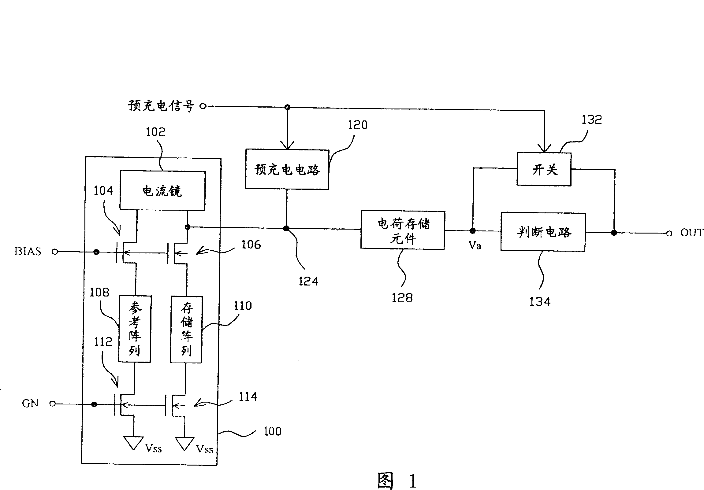
[0058] 1 shows an embodiment of the present invention, wherein a memory circuit 100 includes a current mirror 102, a reference array 108, and a memory array 110. Signal BIAS switches transistors 104 and 106 to connect reference array 108 and memory array 110 to current mirror 102, respectively. Signal BIAS GN is an enabling signal for data reading. The reference terminal of the current mirror 102 is connected to the transistor 104, and the transistor 112 is controlled by the signal GN to connect the reference array 108 to the supply voltage Vss. The mirror terminal of the current mirror 102 is connected to the transistor 106 via the sensing node 124 , and the transistor 114 is controlled by the signal GN to connect the memory array 110 to the power supply voltage Vss. The pre-charging circuit 120 is coupled to the sensing node 124 , the sensing node 124 is also connected to the charge storage element 128 , and the charge storage element 128 is connected to the determination ci...


PUM


Abstract

The invention is a sensing circuit which uses high speed charge shift method when reading data in memory, which is used to sense the voltage change of data inputting port, it realizes high speed sensing according to the difference of charge shifting quantity in precharging period and data read period.

Description

technical field [0001] The present invention relates to a high-speed sensing circuit for memory, in particular to a sensing circuit that utilizes charge transfer technique to increase the rate of reading internal data of memory. Background technique [0002] The data reading of the semiconductor memory is achieved by using a voltage sense amplifier (voltage sense amplifier) ​​or a current sense amplifier (current sense amplifier). The principle of the voltage sense amplifier is to sense the voltage change of the sensing node of the memory during data reading to determine the logic value of the data. Unfortunately, in high-speed devices, data reading is prone to errors due to process variations or deviations, resulting in abnormal operation of the system. Contents of the invention [0003] The present invention proposes a method for detecting the charge difference generated by the charge transfer of different paths, so as to achieve the purpose of high-speed sensing. Beca...

Claims


Application Information

Patent Timeline
Patent Type & Authority Patents(China)
IPC IPC(8): G11C7/06G11C11/4091F25B41/04F25C1/10F25C5/10
CPCF25C5/10F25C1/10F25B41/046
Inventor 唐春安孙毓懋
Owner ELAN MICROELECTRONICS CORPORATION
Features
  • R&D
  • Intellectual Property
  • Life Sciences
  • Materials
  • Tech Scout
  • Unparalleled Data Quality
  • Higher Quality Content
  • 60% Fewer Hallucinations
Learn More