
Semiconductor device

A semiconductor and connection device technology, which is applied in the manufacture of semiconductor devices, hoisting devices, semiconductor/solid-state devices, etc., can solve the problems of hindering high-speed operation, delaying the export of carriers, etc., and achieve the goal of seeking high speed and suppressing the extraction time The effect of deviation

Inactive Publication Date: 2008-08-20
SANYO ELECTRIC CO LTD
View PDF5 Cites 0 Cited by
  • Summary
  • Abstract
  • Description
  • Claims
  • Application Information

AI Technical Summary

Problems solved by technology

When the transistor is turned off, the derivation of minority carriers in the base region is delayed, which constitutes a cause that hinders high-speed operation

Method used


Image

  • Semiconductor device
  • Semiconductor device
  • Semiconductor device

Examples


Embodiment Construction

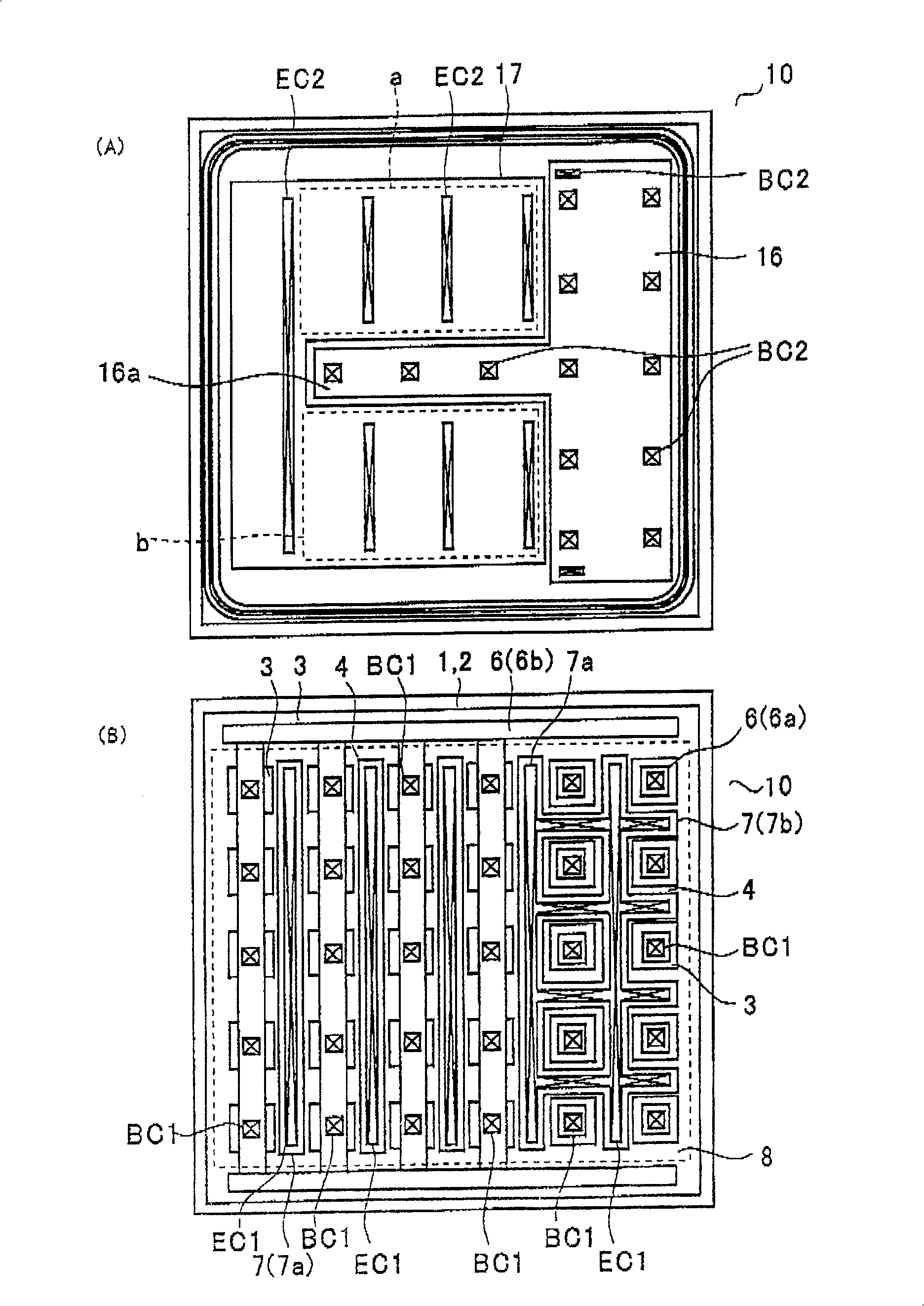
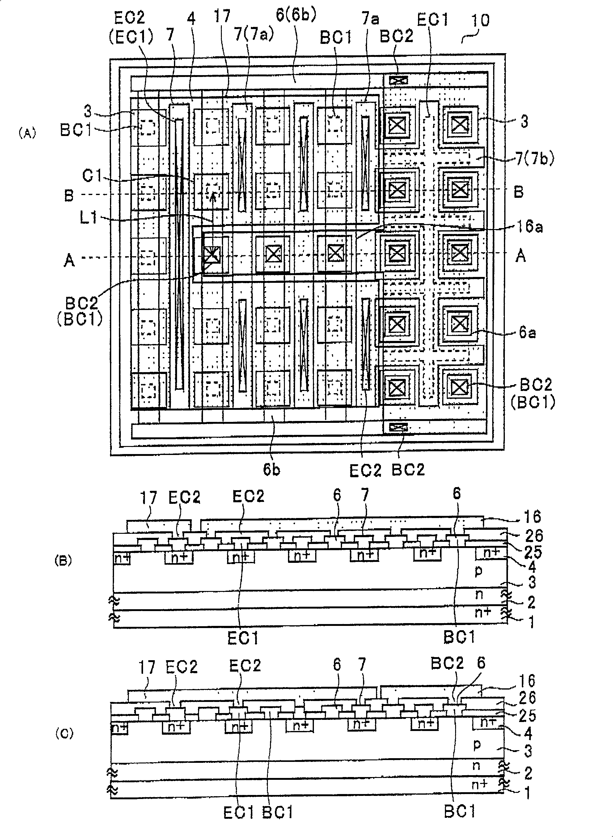
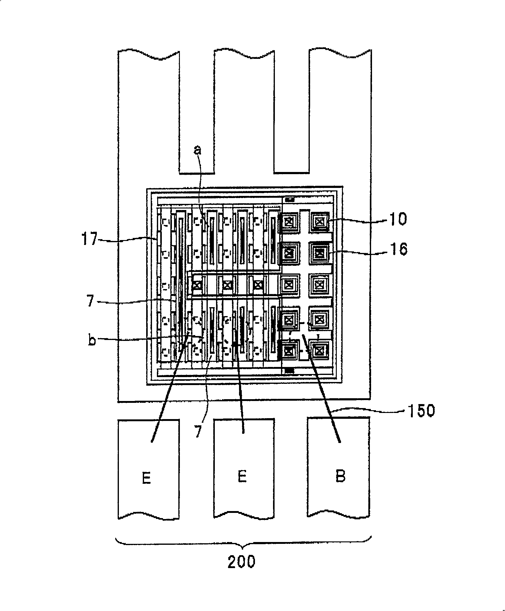
[0068] refer to Figure 1 ~ Figure 3 , taking an npn type bipolar transistor as an example to describe the embodiment of the present invention in detail.

[0069] figure 1 The structure of the semiconductor device 10 as an embodiment of the present invention is shown. figure 1 (A) is a plan view showing the second layer electrode structure, figure 1 (B) is a plan view showing the electrode structure of the first layer and the diffusion region.

[0070] The npn-type bipolar transistor 10 of this embodiment consists of a collector region 2, a base region 3, an emitter region 4, a first base electrode 6, a first emitter electrode 7, a second base electrode 16, a second emitter pole electrode 17 and the protruding portion 16a of the second base electrode.

[0071] The semiconductor substrate 1 is a high-concentration n + -type semiconductor substrate on which, for example, an n-type epitaxial layer or the like is grown to provide a collector region 2 .

[0072] The base re...


PUM


Abstract

PROBLEM TO BE SOLVED: To solve the problem, wherein the distance up to the second base electrode of the base region, near the center of a second emitter electrode, is large and drawing of carrier is delayed in a semiconductor device, including a ladder-shaped first base electrode, a narrow and longer first emitter electrode, a flat type second base electrode, and a second emitter electrode in which the bonding region can be ensured and the wire-bonding location is effectively arranged for the first emitter electrode.SOLUTION: In the semiconductor device wherein a base and an emitter terminals are guided to a side of chip, the flat second emitter electrode is provided, and the first emitter electrode is extended vertically for the chip side where an external terminal is allocated; and a projected part of the second base electrode is provided near the center of the second emitter electrode. Accordingly, the base region of the cell near the center of the second emitter electrode can be provided adjacent to the second base electrode. Consequently, emitter resistance can be lowered, and drawing rate of the carrier of the base region can be improved.

Description

technical field [0001] The present invention relates to a semiconductor device, and more particularly, to a semiconductor device in which the distance from an electrode to be wire-bonded to a base region of an element is reduced to realize an increase in transistor speed. Background technique [0002] refer to Figure 4 , taking an npn transistor as an example to illustrate an existing semiconductor device. [0003] Figure 4 (A) is a schematic diagram of the whole semiconductor element 100, Figure 4 (B) is a plan view of the electrode structure of the first layer, and the dotted line is the electrode of the second layer, Figure 4 (C) is Figure 4 (B) C-C line profile. [0004] For example, an n-type epitaxial layer or the like is stacked on an n + -type silicon semiconductor substrate 51 to provide a collector region 52 . A base region 53 as a p-type impurity region is provided on the surface of the collector region 52 , and an n+ type impurity is diffused on the surface...

Claims


Application Information

Patent Timeline
Patent Type & Authority Patents(China)
IPC IPC(8): H01L29/72H01L29/732H01L29/41H01L29/417H01L21/331
CPCH01L2224/49171H01L2924/1305H01L2924/00B66D5/30H02P21/04H02P27/06
Inventor 赤木修
Owner SANYO ELECTRIC CO LTD
Learn More