
Level shift circuit and semiconductor integrated circuit having the same

A technology for converting circuits and levels, which is applied in the direction of logic circuit connection/interface layout, logic circuit coupling/interface using field effect transistors, electrical components, etc., which can solve problems such as reliability degradation and achieve power consumption reduction and power saving The effect of consumption

Inactive Publication Date: 2007-01-17
PANASONIC CORP
View PDF1 Cites 2 Cited by
  • Summary
  • Abstract
  • Description
  • Claims
  • Application Information

AI Technical Summary

Problems solved by technology

Furthermore, there is a problem that when the drains of the Nch MOS transistors Tn3, Tn4 are directly connected to the high-voltage power supply VDDH, due to the manufacturing process of the semiconductor element, the back gate (back gate) and the drain of these Nch MOS transistors Tn3, Tn4 must be adjusted. poles are reverse-biased by the magnitude of the high supply voltage VDDH, so their reliability is degraded

Method used


Image

  • Level shift circuit and semiconductor integrated circuit having the same
  • Level shift circuit and semiconductor integrated circuit having the same
  • Level shift circuit and semiconductor integrated circuit having the same

Examples


Embodiment 1

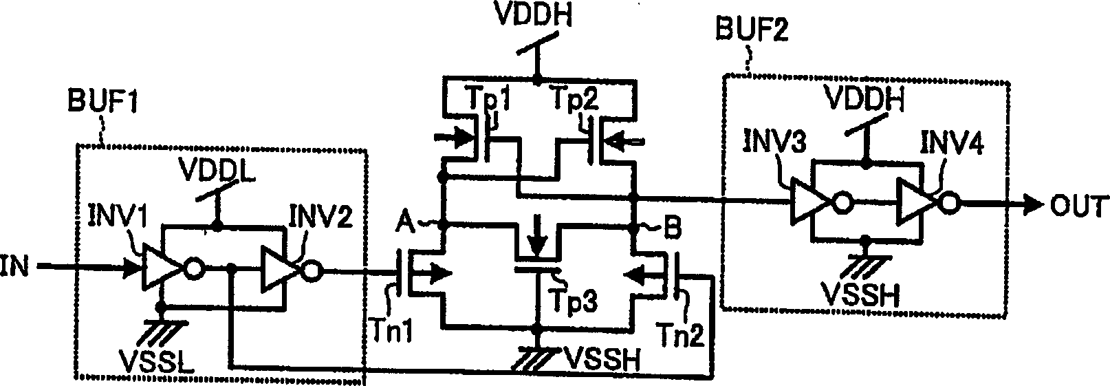
[0041] figure 1 is a configuration diagram showing a level conversion circuit according to Embodiment 1 of the present invention.

[0042] exist figure 1 Among them, BUF1 is a buffer on the input side of the inverters INV1, INV2 that operates at a low supply voltage VDDL and ground (0V) VSSL for this voltage; BUF2 is a buffer that operates at a high supply voltage VDDH and includes inverters Buffers on the output side of phasers INV3 and INV4. The circuit configuration of these buffers BUF1 and BUF2 is only required to have a buffer function, and does not need to be a circuit in which a multistage inverter is connected.

[0043] In addition, in figure 1 Among them, Tn1 and Tn2 are the first and second Nch MOS transistors. Its source is connected to the ground (0V) VSSH for the above-mentioned high-voltage power supply VSSH. Tp1 and Tp2 are the first and second P-channel Pch MOS transistors, the sources of which are connected to the above-mentioned high-voltage power su...

Embodiment 2

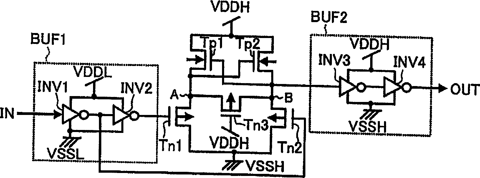
[0057] Next, a level conversion circuit according to Embodiment 2 of the present invention will be described.

[0058] figure 2 The configuration of the level conversion circuit of the second embodiment is shown. figure 2 The level-shifting circuit shown with the figure 1 The level shifting circuit differs in that the figure 1 The transistor constituting the resistor is a Pch MOS transistor Tp3, and in this embodiment, it is composed of an Nch MOS transistor Tn3. Specifically, the source of the Nch MOS transistor (resistor) Tn3 is connected to the node A, the drain is connected to the node B, the gate is connected to the high-voltage power supply VDDH, and is always on.

[0059] Therefore, also in this embodiment, the same effect as that of the above-mentioned embodiment 1 is obtained.

Embodiment 3

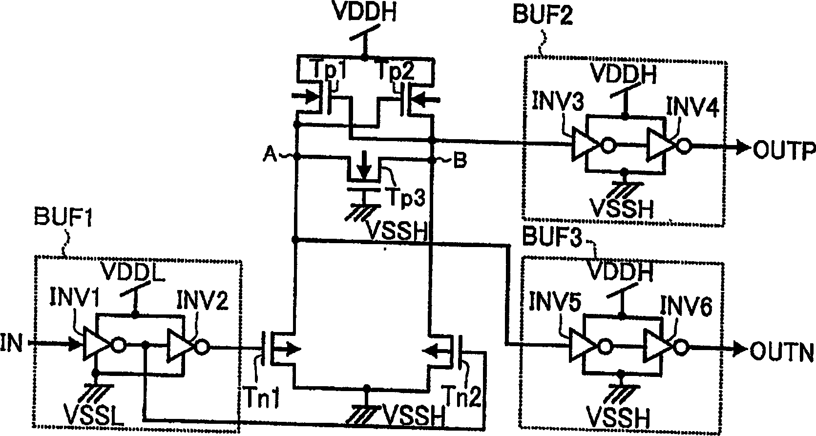
[0061] Next, a level conversion circuit according to Embodiment 3 of the present invention will be described.

[0062] image 3 The configuration of the level conversion circuit of the third embodiment is shown. image 3 The level-shifting circuit shown makes the output signal a differential output signal, with figure 1 The level shifting circuit differs in that, compared to the figure 1 The level conversion circuit is further configured with a buffer BUF3 on the output side.

[0063] The buffer BUF3 on the output side includes two inverters INV5 and INV6 that operate under the high power supply voltage VDDH and the corresponding low power supply voltage VSSH, and the previous stage inverter INV5 is connected to the node A. The output sides of the two buffers BUF2 and BUF3 on the output side are respectively connected to the output terminal OUTP that outputs a signal that is in phase with the input signal IN, and the output terminal OUTN that outputs a signal that is inve...


PUM


Abstract

A level shift circuit comprises two N-ch transistors Tn1,Tn2 that receive a pair of complementary input signals; and two P-ch transistors Tp1,Tp2 that have their gate terminals cross-coupled to each other; wherein nodes A,B, which are the drains of the two N-ch transistors Tn1,Tn2 and which operate inversely to each other, are connected to each other at a resistor Tp3. The resistor Tp3, which comprises a P-ch transistor, has its gate grounded and is always conductive. For example, when the N-ch transistor Tn1 is turned on and the N-ch transistor Tn2 is turned off, a current initially flows from the node A exhibiting a higher potential through the resistor Tp3 to the node B exhibiting a lower potential, which results in a rise of the potential at the node B. Therefore, the potential rise at the node B is promoted as compared with a case where only the P-ch transistor Tp2 is turned on. Thus, the level shift circuit having a less number of elements can operate in a higher rate.

Description

technical field [0001] The present invention relates to a level shift circuit required in semiconductor integrated circuits having different power supply voltages. Background technique [0002] Next, a conventional level conversion circuit will be described. [0003] Figure 5 Indicates a conventional level conversion circuit. exist Figure 5 Among them, BUF1 is a buffer including inverters INV1 and INV2 working at a low power supply voltage, and BUF2 is a buffer including inverters INV3 and INV4 working at a high power supply voltage; VDDH is a high-voltage power supply , VDDL is the low-voltage power supply; VSSH is the ground (0V) for the high-voltage power supply, VSSL is the ground (0V) for the low-voltage power supply; Tn1 is the 1st N-channel (hereinafter referred to as Nch) MOS transistor, Tn2 is the 2nd N Channel (hereinafter referred to as Nch) MOS transistor; Tp1 is the first P channel (hereinafter referred to as Pch) MOS transistor, Tp2 is the second P channel ...

Claims


Application Information

Patent Timeline
Patent Type & Authority Applications(China)
IPC IPC(8): H03K19/0185
CPCH03K3/35613H03K3/012
Inventor 松下刚
Owner PANASONIC CORP
Learn More