Active matrix display device and manufacturing method of the same
A display device and active matrix technology, applied in semiconductor/solid-state device manufacturing, optics, instruments, etc., can solve the problems of increasing manufacturing costs, prevent the increase of manufacturing costs, prevent the reduction of reliability, and increase the bonding strength Effect
- Summary
- Abstract
- Description
- Claims
- Application Information
AI Technical Summary
Problems solved by technology
Method used
Image

Examples
Embodiment Construction
[0029] Preferred embodiments of the active matrix liquid crystal display device of the present invention will be described based on the embodiments.
[0030] (first implementation)
[0031] will first refer to Figures 3 to 9 An active matrix liquid crystal display device and a manufacturing method thereof according to a first embodiment of the present invention will be described.
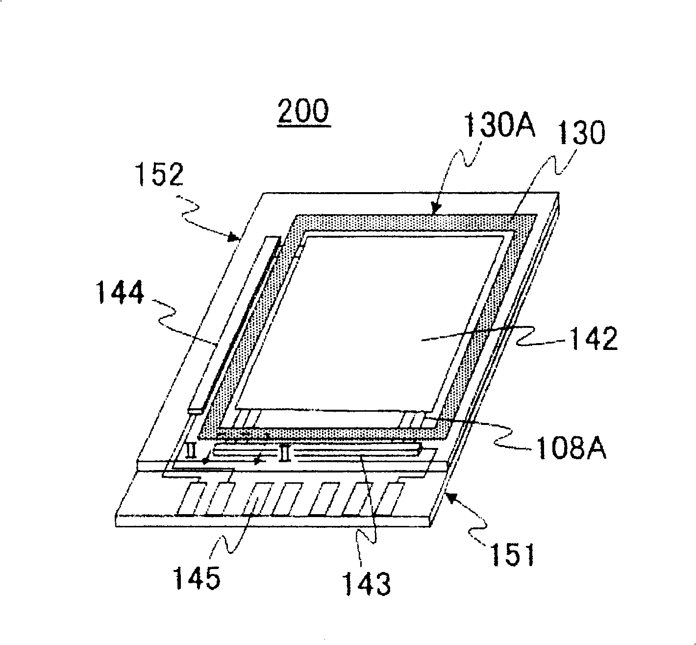
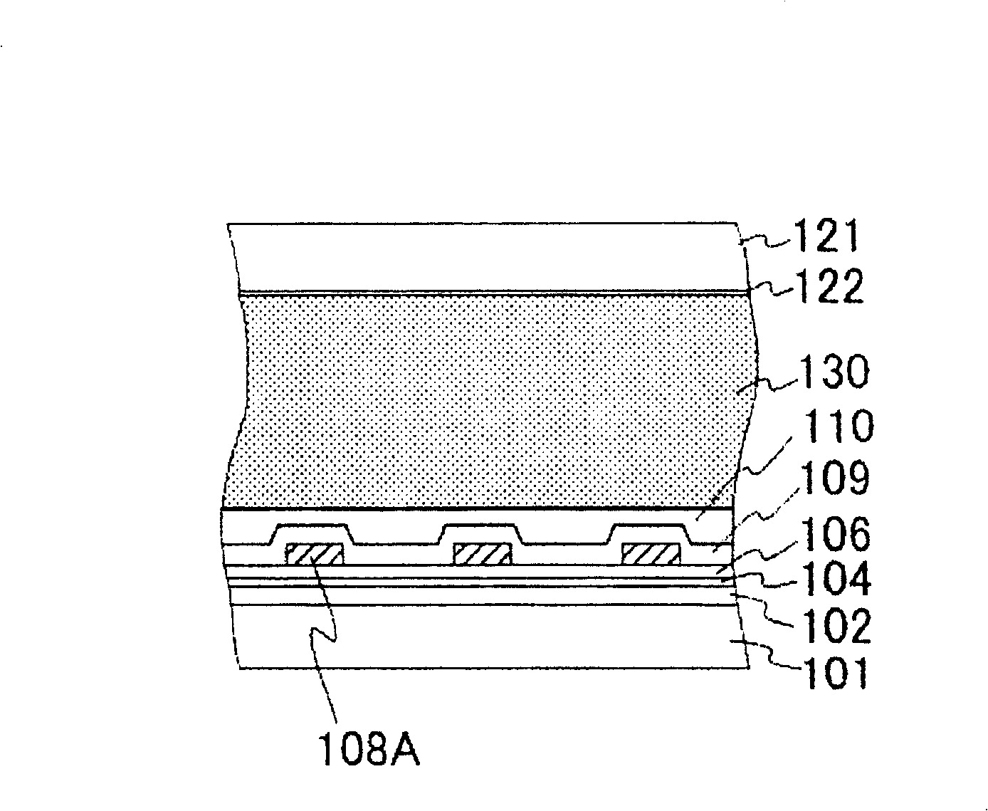
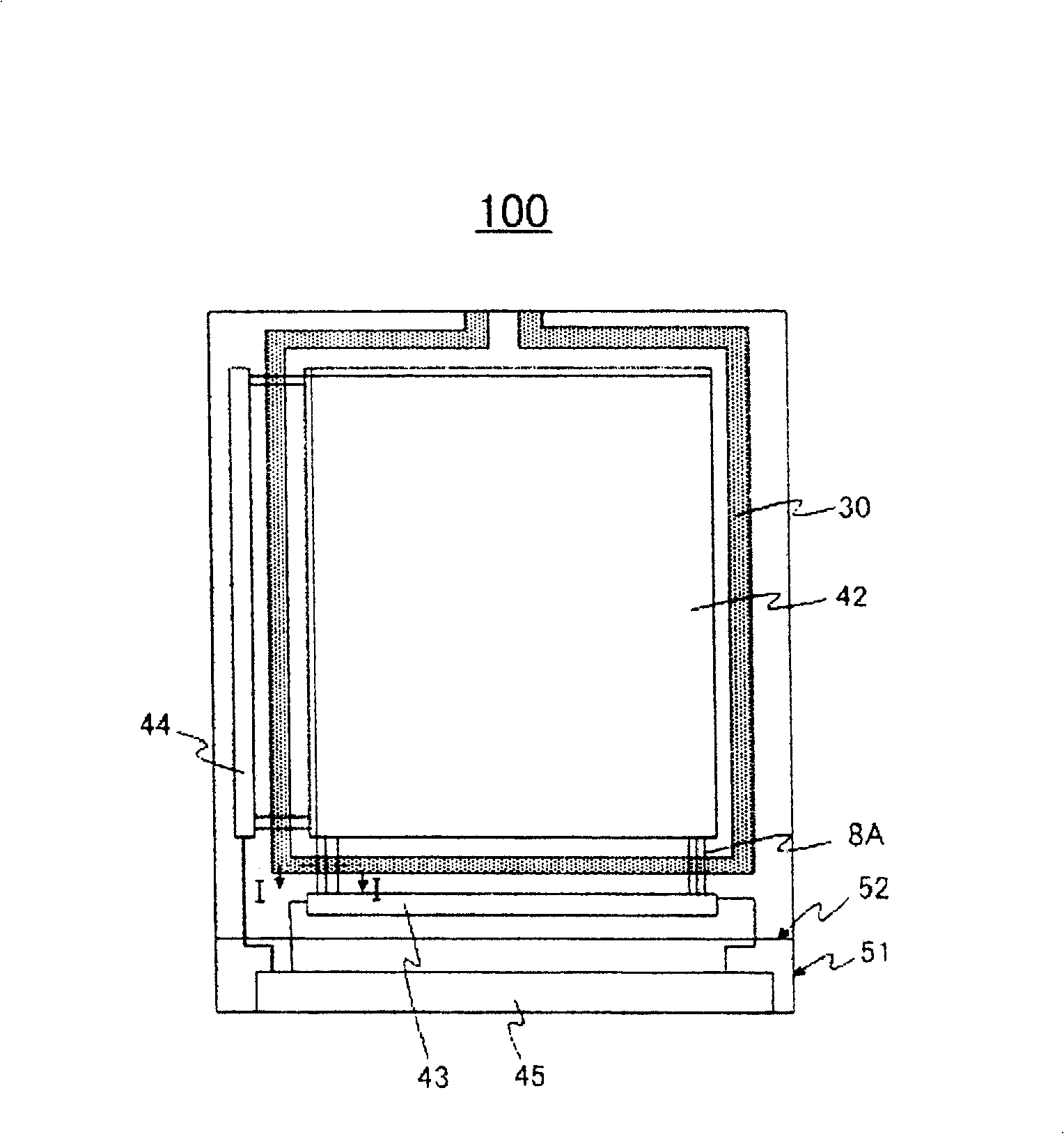
[0032] Such as image 3 As shown in , the active matrix liquid crystal display device 100 includes a TFT substrate 51 in which switching elements (such as TFTs) are formed and an opposite substrate 52 disposed facing the TFT substrate 51 . These substrates are bonded together with a sealing material 30 . A liquid crystal material (not shown) is placed in the area surrounded by the sealing material 30 . The TFT substrate 51 includes a display area in which pixels are formed in a matrix, and circuit units such as a horizontal driver 43 and a vertical driver 44 for driving the pixels. Furthermore,...
PUM
 Abstract
Description
Claims
Application Information
 - R&D
- Intellectual Property
- Life Sciences
- Materials
- Tech Scout
- Unparalleled Data Quality
- Higher Quality Content
- 60% Fewer Hallucinations
Browse by: Latest US Patents, China's latest patents, Technical Efficacy Thesaurus, Application Domain, Technology Topic, Popular Technical Reports.
© 2025 PatSnap. All rights reserved.Legal|Privacy policy|Modern Slavery Act Transparency Statement|Sitemap|About US| Contact US: help@patsnap.com