Semiconductor device and method of manufacturing same
A semiconductor and device technology, applied in the field of silicon-on-insulator materials, can solve problems such as lateral pnp transistor misoperation, and achieve the effect of eliminating misoperation
- Summary
- Abstract
- Description
- Claims
- Application Information
AI Technical Summary
Problems solved by technology
Method used
Image

Examples
Embodiment Construction
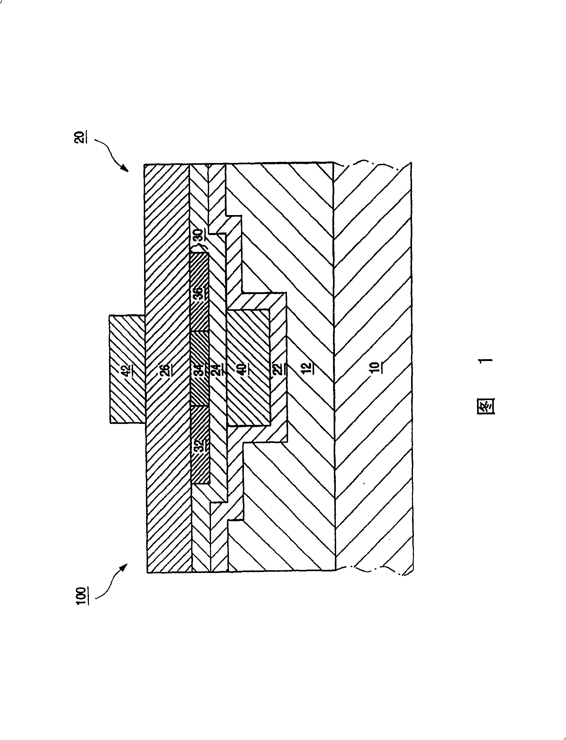
[0025] As shown in the embodiment of FIG. 1, the present invention provides a semiconductor device in the form of an SOI device 100 comprising an insulating layer 10 of dielectric material and a silicon substrate 20 disposed on the insulating layer 10. As shown in FIG. Integrated in this silicon substrate 20 is an element in the form of a bipolar pnp transistor 30, which element has a lightly doped region (in the form of an n-doped region 34) in its central region, while in each of the two lateral regions Inside one is a highly doped region (in the form of P-doped regions 32 and 36 respectively). As shown in FIG. 1, the silicon substrate 20 containing the components 30 is fixed on the insulating layer 10 by means of a fixing medium in the form of an adhesive layer 12 .
[0026] Between the insulator 10 and the n-doped region 34 of the pnp transistor 30, a planar first metallization region (in the form of a first field plate 40) is formed to serve as the lead layer of the pnp t...
PUM
 Abstract
Description
Claims
Application Information
 - R&D Engineer
- R&D Manager
- IP Professional
- Industry Leading Data Capabilities
- Powerful AI technology
- Patent DNA Extraction
Browse by: Latest US Patents, China's latest patents, Technical Efficacy Thesaurus, Application Domain, Technology Topic.
© 2024 PatSnap. All rights reserved.Legal|Privacy policy|Modern Slavery Act Transparency Statement|Sitemap