Method for controlling chip temperature in reaction chamber for semiconductor etching process

A reaction chamber and semiconductor technology, applied in semiconductor/solid-state device manufacturing, electrical components, circuits, etc., can solve the problems of silicon wafer temperature rise, rise to 80 °C, and silicon wafer etching effect deviating from the expected value. The effect of the eclipse effect

Active Publication Date: 2008-12-17
BEIJING NAURA MICROELECTRONICS EQUIP CO LTD
View PDF4 Cites 0 Cited by
  • Summary
  • Abstract
  • Description
  • Claims
  • Application Information

AI Technical Summary

Problems solved by technology

[0003] During the process, the temperature of the silicon wafer needs to be kept at 60°C to 70°C, but during the process, the plasma bombards the silicon wafer, causing the temperature of the silicon wafer to rise, up to 80°C, which will cause silicon The effect of chip etching deviates from the expected value

Method used


Image

  • Method for controlling chip temperature in reaction chamber for semiconductor etching process
  • Method for controlling chip temperature in reaction chamber for semiconductor etching process
  • Method for controlling chip temperature in reaction chamber for semiconductor etching process

Examples


Embodiment Construction

[0021] The following examples are used to illustrate the present invention, but not to limit the scope of the present invention.

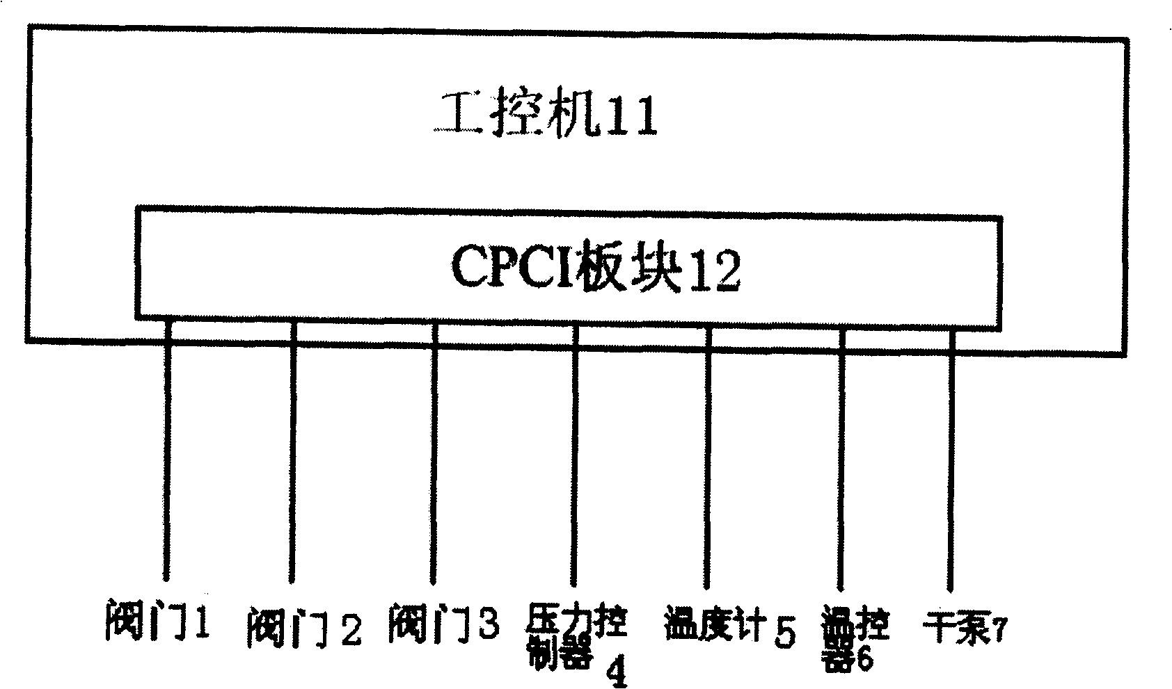
[0022] The connection diagram of the computer control equipment of the present invention is as follows figure 1 As shown, in the wafer etching process, the industrial computer 11 is connected to various controlled devices through the CPCI (Compact Peripheral Component Interconnect) block 12, including valve 1, valve 2, valve 3, and pressure controller 4. , Thermometer 5, Thermostat 6, Dry pump 7.

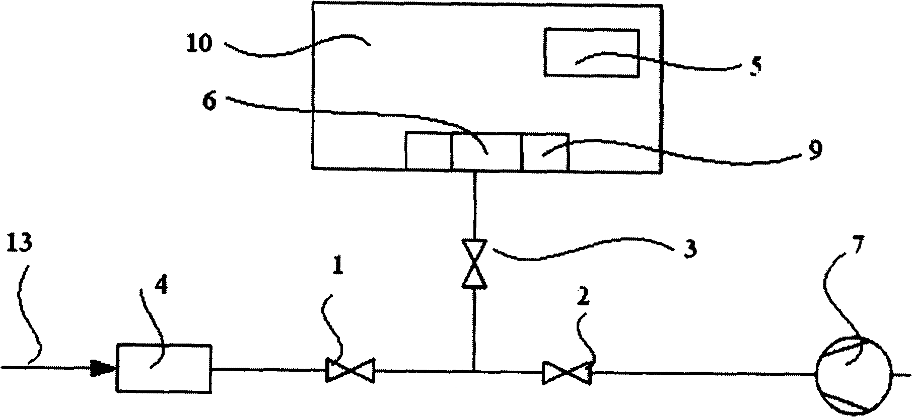
[0023] Such as figure 2 As shown, the electrostatic chuck 9 and the thermometer 5 are placed in the reaction chamber 10. The thermometer 5 can measure the temperature of the reaction chamber 10 in real time. The thermostat 6 is placed at the entrance of the reaction chamber 10, and the gas enters the reaction chamber. At 10 o'clock, the temperature will be heated by the thermostat 6 to a predetermined value.

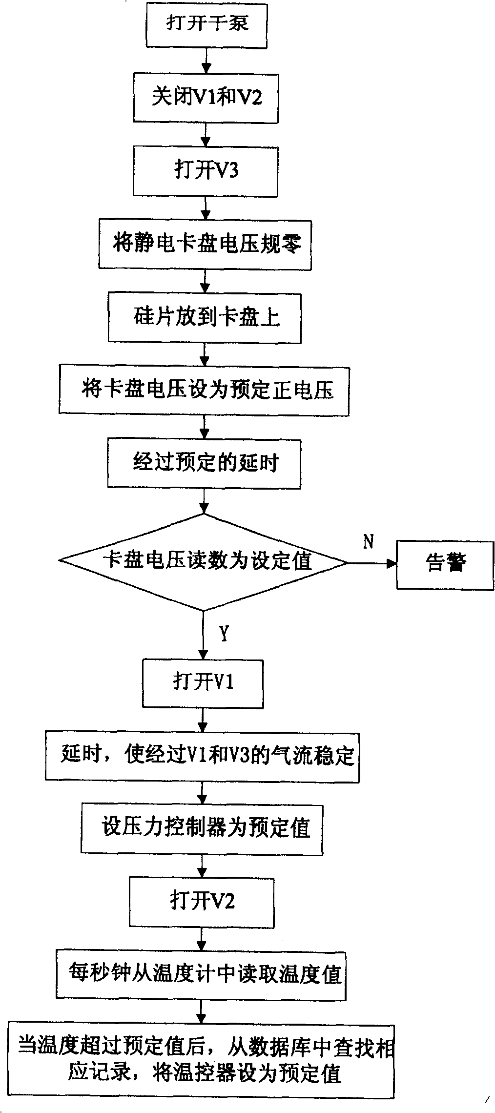
[0024] Such as image 3 As shown, at the beginn...


PUM


Abstract

The invention relates to the field of semiconductor etching. The invention is a method for controlling the wafer temperature of a reaction chamber in a semiconductor etching process. The method of the invention obtains a correspondence between the chamber temperature and the temperature controller on the basis of experiments. Relationship, that is to record, when the temperature of the chamber rises, the temperature of the thermostat needs to be adjusted correspondingly, so as to keep the temperature of the silicon wafer within the normal value range. Save these corresponding relationships in a database. During the process, according to the change of the chamber temperature, search the database, adjust the temperature of the thermostat in real time, so as to control the temperature of the silicon wafer; due to the above technical scheme, the system can be based on The temperature of the reaction chamber changes, the database is searched in real time, and the temperature of the thermostat is adjusted in real time, thereby controlling the temperature of the silicon wafer at a normal value and improving the etching effect of the wafer.

Description

Technical field [0001] The invention relates to the field of semiconductor etching, in particular to a method for controlling the temperature of a wafer in a reaction chamber in a semiconductor etching process. Background technique [0002] During the silicon wafer etching process, the silicon wafer needs to be fixed on the electrostatic chuck to maintain the stability of the silicon wafer during the process; at the same time, the temperature of the silicon wafer can be achieved only when the silicon wafer is fixed on the electrostatic chuck Control, make the silicon wafer get uniform heating or cooling. The fixing of the silicon wafer is realized by applying a positive voltage to the electrostatic chuck; the temperature control of the silicon wafer is realized by the thermostat on the electrostatic chuck and the flow of gas, which can ensure that the silicon wafer is heated evenly and at the same time The silicon wafer reaches the target temperature the fastest. [0003] During ...

Claims


Application Information

Patent Timeline
Patent Type & Authority Patents(China)
IPC IPC(8): C23F4/04H01L21/3065
Inventor 张京华
Owner BEIJING NAURA MICROELECTRONICS EQUIP CO LTD
Why Eureka
Try Eureka