

Semiconductor integrated circuit
A technology of semiconductors and constant current circuits, applied in the manufacture of semiconductor devices, circuits, and semiconductor/solid-state devices, etc., can solve the problems of different currents, voltages, wiring resistance values, and difficulty in correctly controlling the current value.
- Summary
- Abstract
- Description
- Claims
- Application Information
AI Technical Summary
Problems solved by technology
Method used
Image

Examples
Embodiment Construction
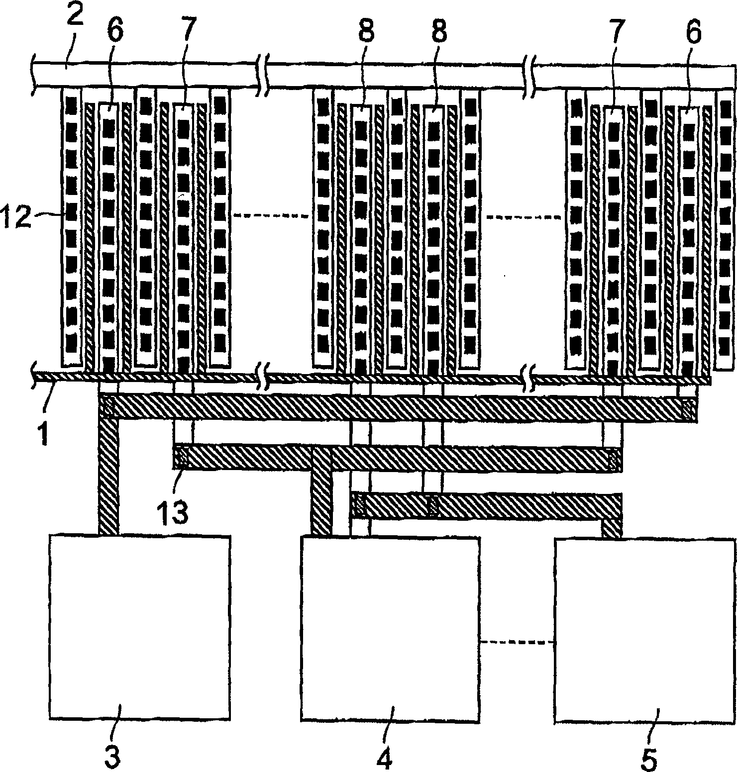
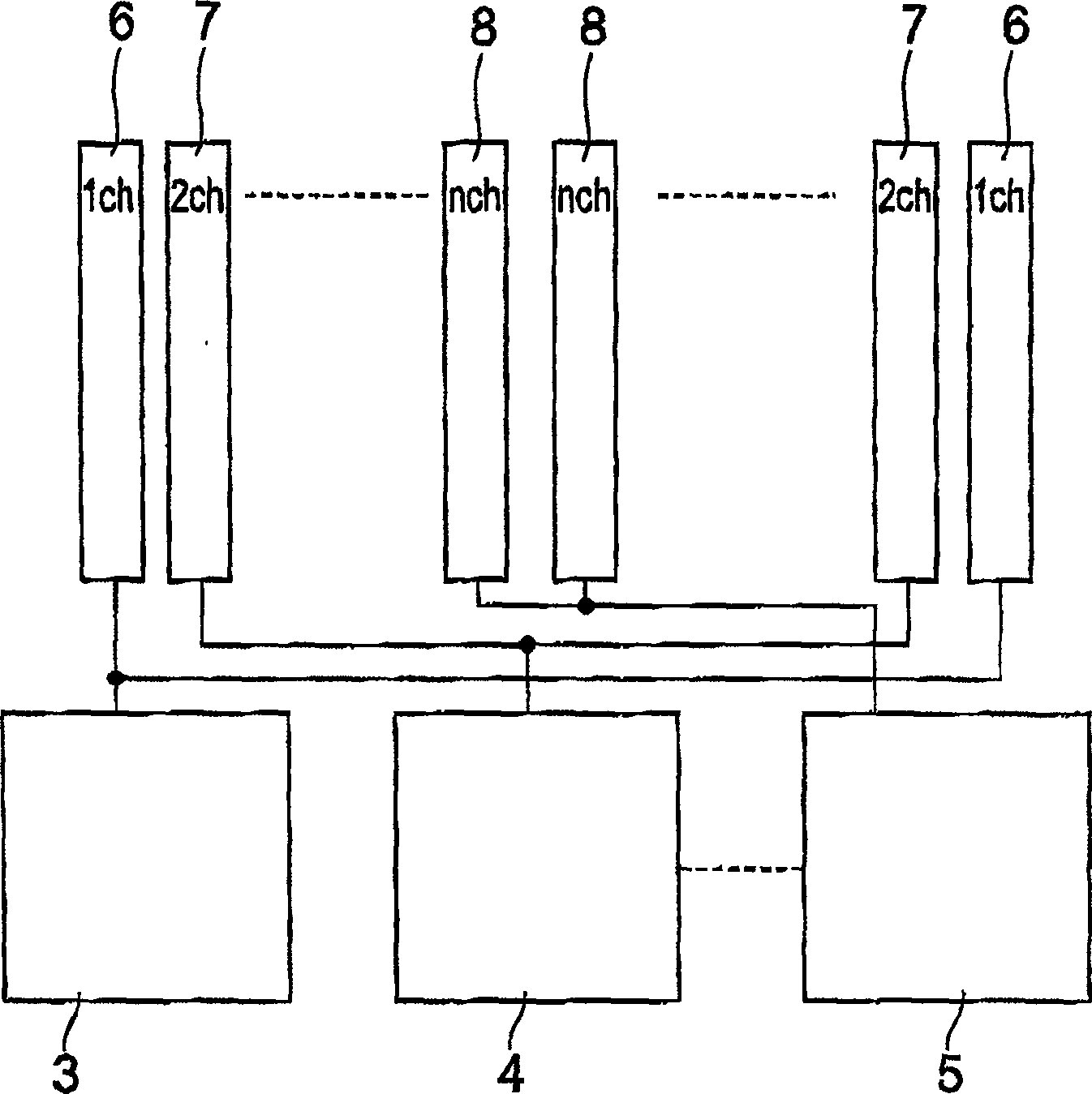
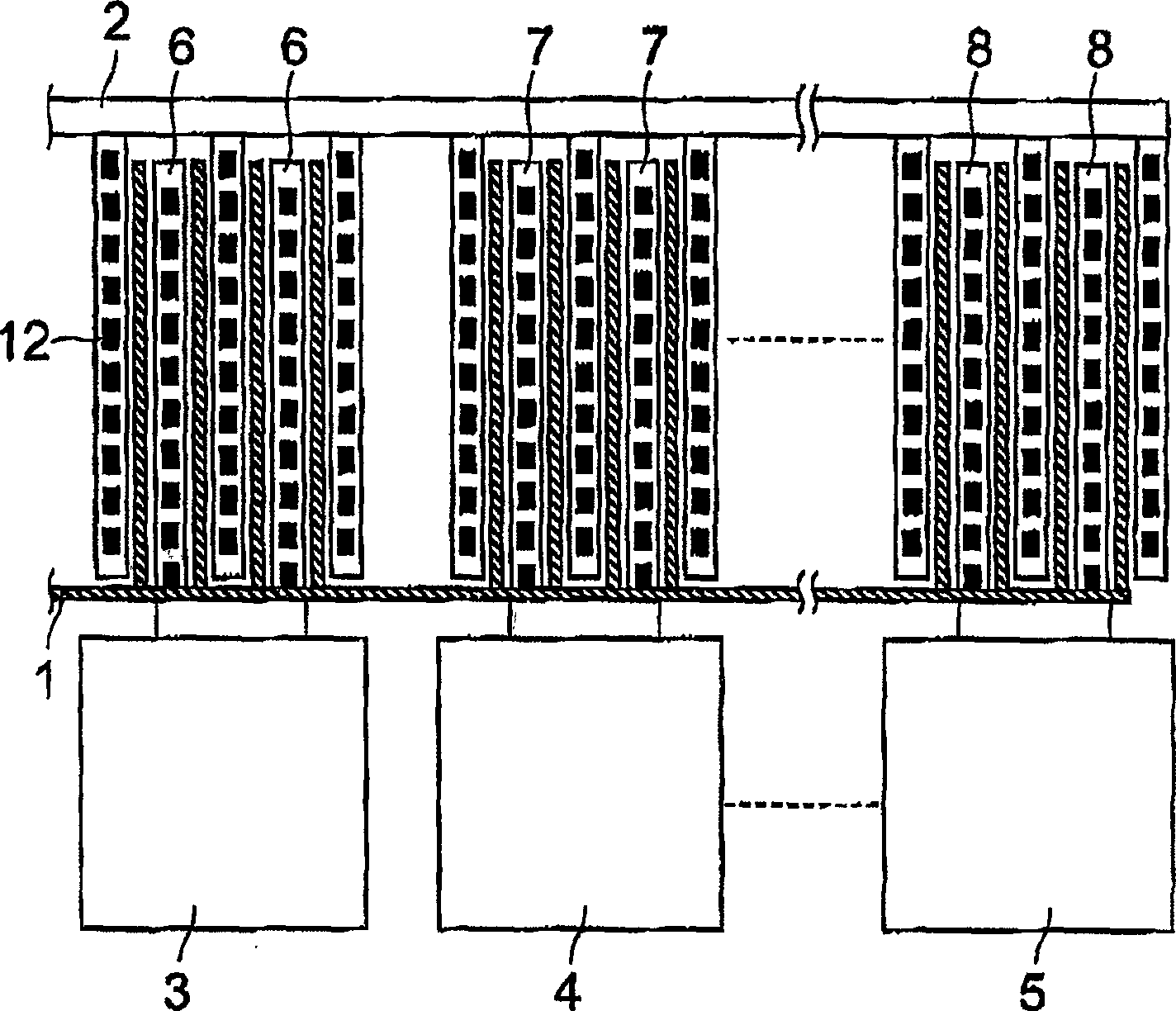
[0019] Embodiments of the present invention will be described below with reference to the accompanying drawings. figure 1 It is a configuration diagram showing the arrangement of constant current elements of the constant current circuit of this embodiment. A gate terminal 1 and a source terminal 2 which are constant current elements of an N-type MOS transistor or a P-type MOS transistor are common to all channels. The branched drain terminals are arranged in sequence from the left end and right end of the gate terminal 1 and source terminal 2 to the center in the order of the first drain terminal 6, the second drain terminal 7, and then the nth drain terminal. . In this way, in the center, the branched N-th drain terminals 8 corresponding to the N-th channel are adjacently arranged. Then, it is connected to the first output terminal channel 3, the second output terminal channel 4, and the Nth output terminal channel 5, which are output terminals of each channel.
[0020] Si...
PUM
 Abstract
Description
Claims
Application Information