High power LED flip-chip and its manufacturing method

A flip-chip, high-power technology, used in semiconductor devices, electrical components, circuits, etc., can solve the problems of lack of work function, difficult to achieve P-GaN doping concentration, etc., and achieve the effect of improving the heat dissipation effect.

Inactive Publication Date: 2009-04-29
EPILIGHT TECH +1
View PDF5 Cites 0 Cited by
  • Summary
  • Abstract
  • Description
  • Claims
  • Application Information

AI Technical Summary

Problems solved by technology

[0006] 2) The traditional LED adopts a positive mounting structure, and the light generated in the active area is emitted from the front through the transparent conductive layer electrode. The main disadvantage is that about 30% of the light is absorbed by the P electrode
In the design process of high-power LED electrodes, both low ohmic contact resistance and high light extraction efficiency must be taken into account. There are two factors that restrict the ohmic contact of P electrodes: one is that the doping concentration of P-GaN is difficult to reach, and holes can tunnel The level of the Schottky barrier; the second is the lack of metals or metal systems with a work function higher than that of P-GaN

Method used


Image

  • High power LED flip-chip and its manufacturing method
  • High power LED flip-chip and its manufacturing method
  • High power LED flip-chip and its manufacturing method

Examples


Embodiment Construction

[0026] The wavelength range of the high-power LED flip chip of the present invention is 430nm-530nm.

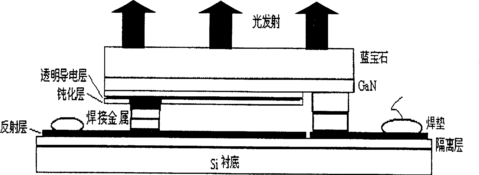
[0027] like figure 1 As shown, the high-power LED flip chip of the present invention is composed of a P-N electrode epitaxial wafer and a silicon substrate with a reflective layer.

[0028] The P-N electrode epitaxial wafer includes a sapphire substrate, and the sapphire substrate has the characteristics of low thermal conductivity and insulation. The N-GaN layer formed on the sapphire substrate, the P-GaN layer and the light-emitting layer formed on the N-GaN layer (the light-emitting layer is located between the N-GaN layer and the P-GaN layer), so as to be compatible with the N-GaN layer make electrical contact.

[0029]For flip-chip LEDs, light is emitted from a transparent sapphire substrate, requiring high light transmittance to the transparent conductive layer. Due to the limited electrical conductivity of the P-GaN layer, a layer is deposited on the surface of the P...


PUM

PropertyMeasurementUnit
thicknessaaaaaaaaaa
thicknessaaaaaaaaaa
thicknessaaaaaaaaaa

Abstract

The invention relates to a high-power LED face-down chip, formed by P-N electrode extending sheet and silicon substrate with reflective layer, wherein the P-N electrodes have inactivate layer between; the characteristic semi-conductive silicon substrate has electric insulated layer above; the metal reflective layer is above the insulated layer; the P-N electrode extending sheet and the silicon substrate with reflective layer are face-down welded to form high-power LED face-down chip. And its production comprises that: on silicon substrate, using PECVD to deposit one layer of P-N electrode electric insulated layer as SiO2 or Si3N4 insulated layer at 50-100nm thick; then using magnetic-control splash or electron beam to evaporate one layer of metal reflective layer at 200-300nm made from TiAl or TiAg. The invention can improve the lighting efficiency and radiation efficiency.

Description

technical field [0001] The invention relates to a method for preparing a high-power LED flip-chip made of gallium nitride (GaN) semiconductor, in particular to a process for evaporating a metal reflection layer on a silicon substrate to improve light extraction efficiency and heat dissipation. Background technique [0002] Luminous efficiency, especially low light extraction efficiency and poor heat dissipation are the main technical bottlenecks faced by high-power LEDs. The light extraction efficiency of traditional front-mounted LEDs is mainly affected by the following factors: 1) The light transmittance of the P-GaN semi-transparent metal contact electrode layer is 70%-80%; 2) The bonding solder joints on the P electrodes and 3) The relative refractive index of the GaN material is relatively high, and the light is reflected and absorbed multiple times between the sapphire and the translucent metal electrode. The above factors lead to the fact that the current LED light e...

Claims


Application Information

Patent Timeline
Patent Type & Authority Patents(China)
IPC IPC(8): H01L33/00H01L33/48H01L33/60H01L33/64
Inventor 靳彩霞董志江许亚兵丁晓民黄素梅
Owner EPILIGHT TECH
Why Eureka
Try Eureka