Insulation layer thickness electric test structure in micro electro-mechanical systems device structure

A technology of insulating layer thickness and micro-electromechanical system, which is applied in the field of electricity and semiconductors, can solve the problems of slow measurement speed and achieve the effect of simple test equipment

Inactive Publication Date: 2009-05-20
NANTONG SHENGYANG ELECTRIC CO LTD +1
View PDF3 Cites 0 Cited by
  • Summary
  • Abstract
  • Description
  • Claims
  • Application Information

AI Technical Summary

Problems solved by technology

Most of the current insulating layer thickness tests use optical or mechanical methods, the measurement speed is slow, and the automatic extraction of the device structure parameter model cannot be realized. Therefore, a fast and effective test method has practical significance

Method used


Image

  • Insulation layer thickness electric test structure in micro electro-mechanical systems device structure
  • Insulation layer thickness electric test structure in micro electro-mechanical systems device structure
  • Insulation layer thickness electric test structure in micro electro-mechanical systems device structure

Examples


Embodiment Construction

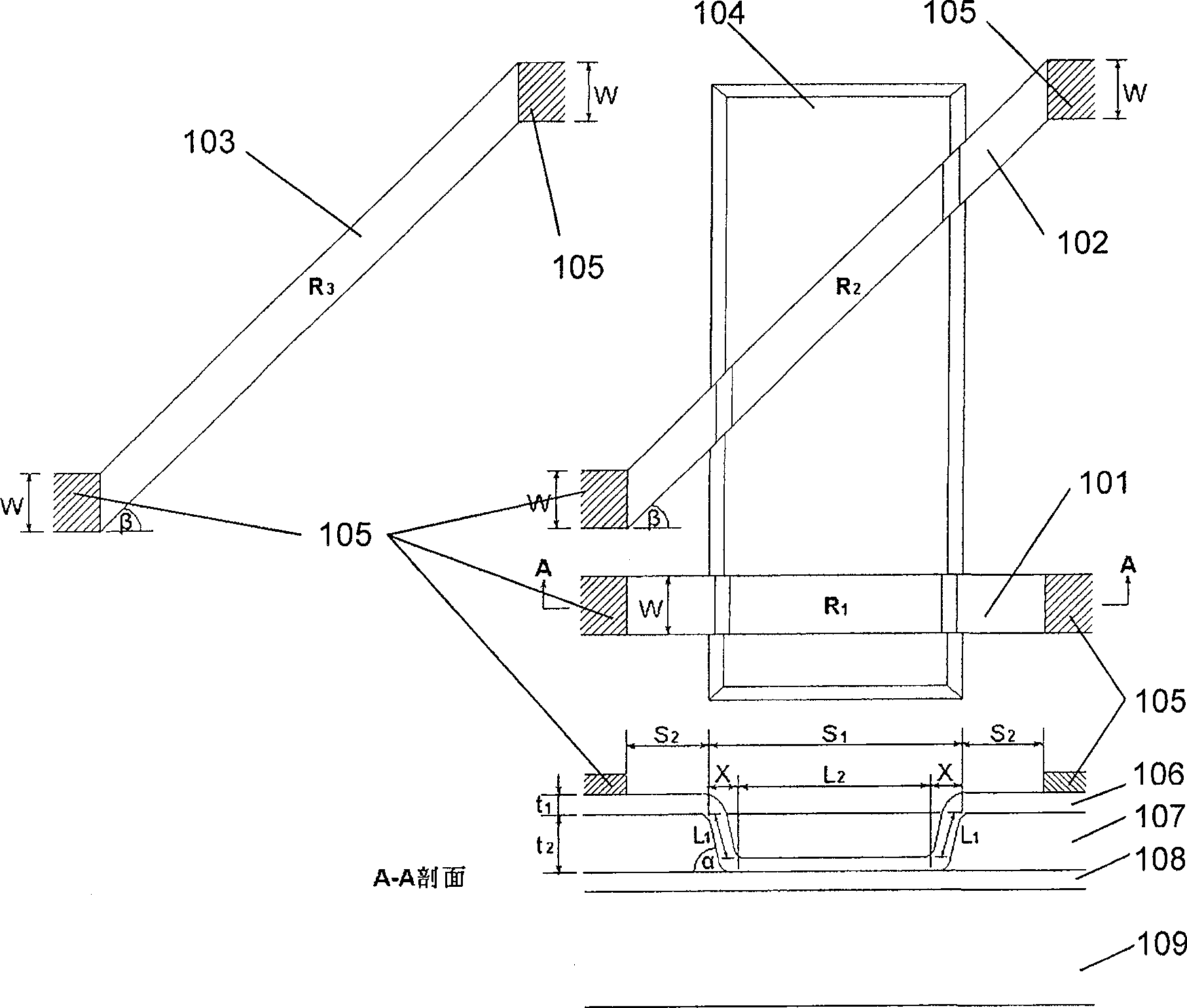
[0010] see figure 1 , in the test structure, 104 is the trench opened on the insulating layer 107, and the thickness of 107 is equal to t 2 , t 2 is the parameter ultimately required by the present invention. It can be seen from the section A-A that the insulating layer 108 whose depth reaches below, 107 and 108 are insulating layer materials with different properties, for example, 108 is silicon nitride, and 107 is silicon dioxide. The width design dimension of the groove 104 is S 1 , length to be able to lay down the polysilicon strip R 1 , R 2 And leave a certain length margin for the design size, such as figure 1 shown. The etched trench 104 usually has a certain angle, that is, the upper and lower widths are different, and the angle is represented by α.

[0011] 106 is polycrystalline silicon material, and its thickness is equal to t 1 . 101 is the polysilicon resistance bar R that polysilicon material 106 is made through photoetching, etching 1 , polysilicon st...


PUM

PropertyMeasurementUnit
thicknessaaaaaaaaaa

Abstract

The invention provides an electric test structure with the surface processing of the thickness of an insulating layer in MEMS device structure, a basic aim is that the thickness value of the insulating layer is gained by the way of electrical measurement. Of the surface process technology, the insulating layer in the MEMS device structure is usually silica, silicon nitride or polymer. The invention utilizes a conductive poly-silicon on the insulating layer material and a groove arranged on the insulating layer to design the electric test structure, and obtains the thickness of the insulating layer by measuring the resistance of poly-silicon strips with introducing a mathematical model.

Description

technical field [0001] The invention relates to a micro-electro-mechanical system (MEMS) device processing technology, in particular to an electrical testing structure for the thickness of an insulating layer in a micro-electro-mechanical system device structure, belonging to the fields of electricity and semiconductors. Background technique [0002] There are multiple layers of insulating materials in the MEMS device structure, such as sacrificial layers made of silicon dioxide and silicon nitride. The thickness of these materials is a very important parameter in the MEMS structure, which directly determines the longitudinal movement range of the movable structure, so Testing and process monitoring of these insulation thicknesses is of great interest. Most of the current insulation layer thickness tests use optical or mechanical methods, the measurement speed is slow, and the automatic extraction of the device structure parameter model cannot be realized. Therefore, a fast ...

Claims


Application Information

Patent Timeline
Patent Type & Authority Patents(China)
IPC IPC(8): G01B7/06B81C5/00B81C99/00
Inventor 李伟华钱晓霞
Owner NANTONG SHENGYANG ELECTRIC CO LTD
Why Eureka
Try Eureka