Different conductive layers alignment error electricity testing structure in micromotor system apparatus process

A technology of alignment error and test structure, applied in microstructure technology, microstructure devices, piezoelectric/electrostrictive/magnetostrictive devices, etc., can solve problems such as registration error extraction, achieve consistent measurement methods, test Simple method and simple test equipment

Inactive Publication Date: 2009-09-23
SOUTHEAST UNIV
View PDF5 Cites 0 Cited by
  • Summary
  • Abstract
  • Description
  • Claims
  • Application Information

AI Technical Summary

Problems solved by technology

At present, electrical parameters, geometric dimension parameters and errors can be extracted by electrical methods, but registration errors cannot be extracted by electrical methods

Method used


Image

  • Different conductive layers alignment error electricity testing structure in micromotor system apparatus process
  • Different conductive layers alignment error electricity testing structure in micromotor system apparatus process
  • Different conductive layers alignment error electricity testing structure in micromotor system apparatus process

Examples


Embodiment Construction

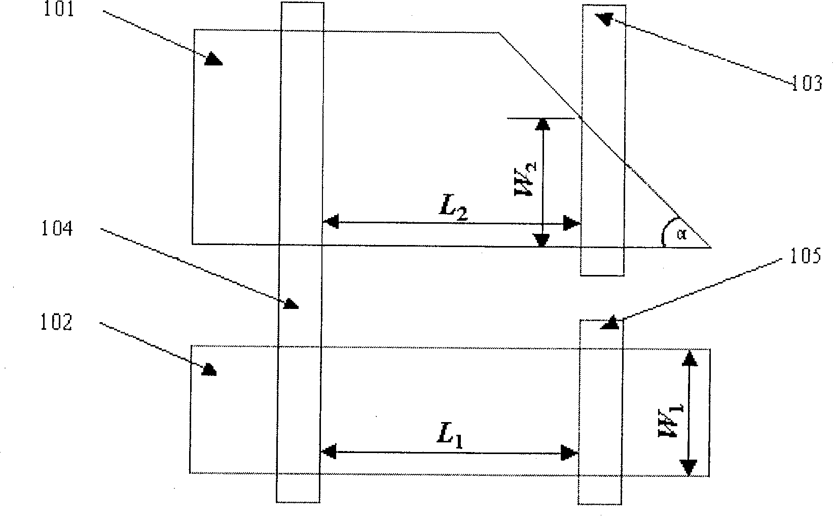
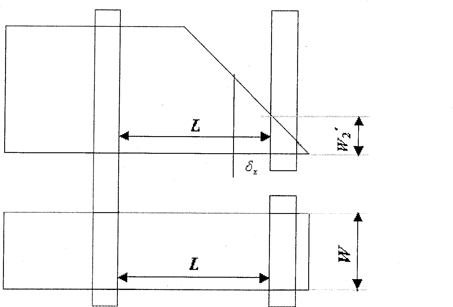
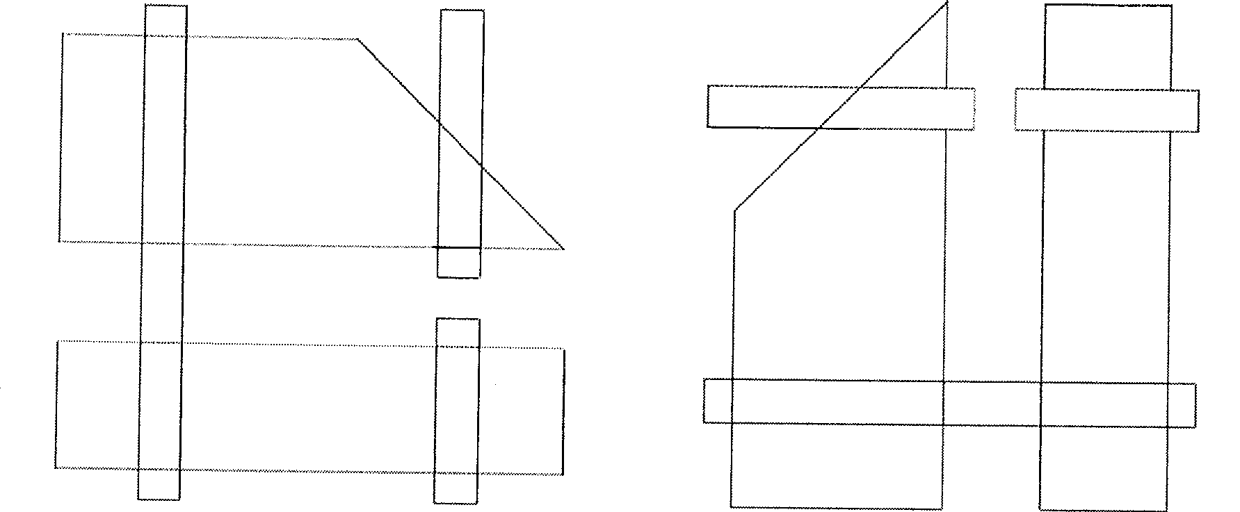
[0016] see figure 1 , in the test structure, 101 is a trapezoid, 102 is a rectangle, the material of these two patterns is a semiconductor material layer, which can be single crystal silicon, or polycrystalline silicon 1, polycrystalline silicon 2, they are all conductive due to doping Of course, there must also be resistivity. 103, 104, and 105 are strip-shaped metal layers. The metal strip and the semiconductor are contacted to form a connection, and the two metal strips 104, 103 (105) and the semiconductor between them jointly form a resistor with a connecting line. Its size is calculated by the following formula:

[0017] R = R S ( L W ) - - - ( 1 )

[0018] Among them, R S is the sheet resistance value of the semiconductor, L is the distance between two...


PUM


Abstract

The invention relates to an electricity test structure for alignment error of different conducting layer graphics in processing of micro-electro-mechanical system components. A metal layer is taken as the base layer to design an alignment error test structure of all conducting layers; in the structure, a semiconductor layer includes two semiconductors which are separated, made in the same material and in different shapes; one of the semiconductors is trapezoidal and the other is rectangular, which are arranged in parallel; the connected metal layer formed includes two paralleled metal bars with spacing, one of which is vertically covered on an upper and a lower bottom sides of the trapezoidal window as well as two long sides of the rectangular window, and the other is covered on the obtuse angle part of the trapezoidal window and two long sides of the rectangular window, and cut off in the separation area between the two semiconductors; the two metal bars and the semiconductors between the metal bars form a resistance with connecting wires; when relative deflection exists between the metal layer graphics and the insulation layer graphics, the testing resistance changes, and the alignment error of the metal layer relative to the semiconductor material graphics can be obtained.

Description

technical field [0001] The invention relates to a micro-electro-mechanical system (MEMS) device processing technology, in particular to an electrical test structure for alignment errors of patterns of different conductive layers in the processing of micro-electro-mechanical devices, belonging to the fields of electricity and semiconductors. Background technique [0002] Multiple layers of conductive material exist in microelectromechanical systems (MEMS) device processing. For example, Silicon Substrate, Poly1, Poly2, and Metal. Since the material layers are successively deposited on the silicon substrate and the processing is also successive overlaying, there is a requirement that the pattern of the subsequent conductive layer be aligned with the pattern of the previous conductive layer. [0003] The traditional overlay alignment is to adopt the method of mutual nesting of large and small graphics, that is, to design the same graphics of different sizes on different layers...

Claims


Application Information

Patent Timeline
Patent Type & Authority Patents(China)
IPC IPC(8): B81C5/00G01B7/00B81C99/00
Inventor 李伟华钱晓霞
Owner SOUTHEAST UNIV
Why Eureka
Try Eureka