Electrically rewritable non-volatile memory element and method of manufacturing the same

A non-volatile storage and component technology, used in electrical components, semiconductor/solid-state device manufacturing, information storage, etc., can solve the problems of recording layer damage, inability to apply electrode protective film, low thermal efficiency, etc., and achieve the effect of reducing the amount of damage

Inactive Publication Date: 2009-05-27
PS4 LUXCO SARL
View PDF6 Cites 0 Cited by
  • Summary
  • Abstract
  • Description
  • Claims
  • Application Information

AI Technical Summary

Problems solved by technology

[0016] The non-volatile memory elements described in the above three documents as well as in USP 5,536,947 thus have the disadvantage of low thermal efficiency due to the large amount of heat released to the metal layer located above the recording layer
[0018] However, in the case of a structure in which only part of the upper surface of the recording layer is in contact with the upper electrode, such as in the nonvolatile memory elements described in Japanese Patent Application Laid-Open Nos. 2004-289029 and 2004-349709, it is impossible to make the upper electrode The electrode acts as a protective film
There is therefore a risk of severe damage to the recording layer occurring during patterning or via formation of the recording layer, as described above

Method used


Image

  • Electrically rewritable non-volatile memory element and method of manufacturing the same
  • Electrically rewritable non-volatile memory element and method of manufacturing the same
  • Electrically rewritable non-volatile memory element and method of manufacturing the same

Examples


Embodiment Construction

[0055] Now, preferred embodiments of the present invention will be explained in detail with reference to the drawings.

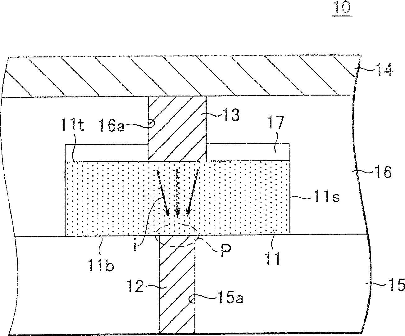
[0056] figure 1 It is a schematic cross-sectional view of the structure of the nonvolatile memory element 10 according to the first preferred embodiment of the present invention.

[0057] Such as figure 1 As shown, the nonvolatile memory element 10 according to the present invention is provided with: a recording layer 11, which includes a phase change material; a lower electrode 12, which is provided in contact with the lower surface 11b of the recording layer 11; and an upper electrode 13 which is in contact with The upper surface 11 t of the recording layer 11 is provided in contact; and the bit line 14 is a metal layer provided on the upper electrode 13.

[0058] The lower electrode 12 is embedded in the through hole 15 a provided to the first interlayer insulating film 15. Such as figure 1 As shown, the lower electrode 12 is in contact with the lower sur...


PUM


Abstract

A non-volatile memory element includes a recording layer that includes a phase change material, a lower electrode provided in contact with the recording layer, an upper electrode provided in contact with a portion of the upper surface of the recording layer, a protective insulation film provided in contact with the other portion of the upper surface of the recording layer, and an interlayer insulation film provided on the protective insulation film. High thermal efficiency can thereby be obtained because the size of the area of contact between the recording layer and the upper electrode is reduced. Providing the protective insulation film between the interlayer insulation film and the upper surface of the recording layer makes it possible to reduce damage sustained by the recording layer during patterning of the recording layer or during formation of the through-hole for exposing a portion of the recording layer.

Description

Technical field [0001] The present invention relates to an electrically rewritable nonvolatile memory element and a method of manufacturing the element. More specifically, the present invention relates to an electrically rewritable nonvolatile memory element having a recording layer including a phase change material and a method of manufacturing the element. Background technique [0002] Hierarchical storage devices are used for personal computers and servers. There are lower-level memories that are cheap and provide high storage capacity, while higher-level memories provide high-speed operation. The bottom level generally consists of magnetic storage such as hard drives and tapes. In addition to non-volatility, magnetic storage is an inexpensive method of storing much larger amounts of information than solid-state devices such as semiconductor memory. However, in contrast to the sequential access operations of magnetic storage devices, semiconductor memories are much faster and ...

Claims


Application Information

Patent Timeline
Patent Type & Authority Patents(China)
IPC IPC(8): H01L45/00H01L27/24H01L21/82G11C16/02
CPCH01L45/143H01L45/1675G11C2213/52H01L27/2436H01L45/1273H01L45/06H01L45/144H01L45/148H01L45/1683H01L45/126H01L45/1233H10B63/30H10N70/8413H10N70/8418H10N70/231H10N70/8825H10N70/884H10N70/8828H10N70/826H10N70/063H10N70/066
Inventor 浅野勇佐藤夏树中井洁
Owner PS4 LUXCO SARL
Why Eureka
Try Eureka