Method for epitaxial growth of gallium antimonide on gallium arsenide substrate

A technology of epitaxial growth and gallium antimonide, which is applied in the direction of electrical components, semiconductor/solid-state device manufacturing, circuits, etc., can solve the problems of high dislocation density, low peak intensity, poor crystal quality, etc., and achieve the reduction of density and screw position The effect of reducing the error density and increasing the strength

Inactive Publication Date: 2009-06-03
INST OF SEMICONDUCTORS - CHINESE ACAD OF SCI
View PDF4 Cites 3 Cited by
  • Summary
  • Abstract
  • Description
  • Claims
  • Application Information

AI Technical Summary

Problems solved by technology

However, there are the following disadvantages: due to the lattice mismatch of about 7% between the GaAs substrate and the GaSb epitaxial layer, GaSb grows in a three-dimensional island shape, and the obtained GaSb material has a rough surface, high dislocation density, and poor crystal quality
[0006] However, the test found that the optical quality of the GaSb epitaxial layer prepared by the double buffer layer process is not good. Errors enter the GaSb epitaxial layer, resulting in a large number of non-radiative recombination centers, and the photogenerated carriers are recombined by these defects before radiative recombination occurs.

Method used


Image

  • Method for epitaxial growth of gallium antimonide on gallium arsenide substrate
  • Method for epitaxial growth of gallium antimonide on gallium arsenide substrate
  • Method for epitaxial growth of gallium antimonide on gallium arsenide substrate

Examples


Embodiment 1

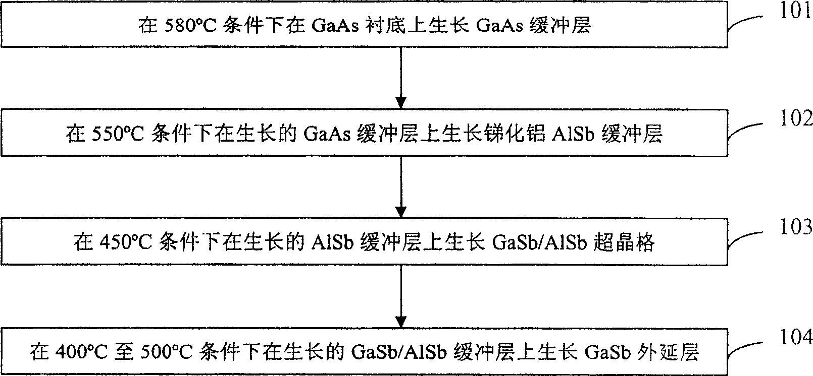
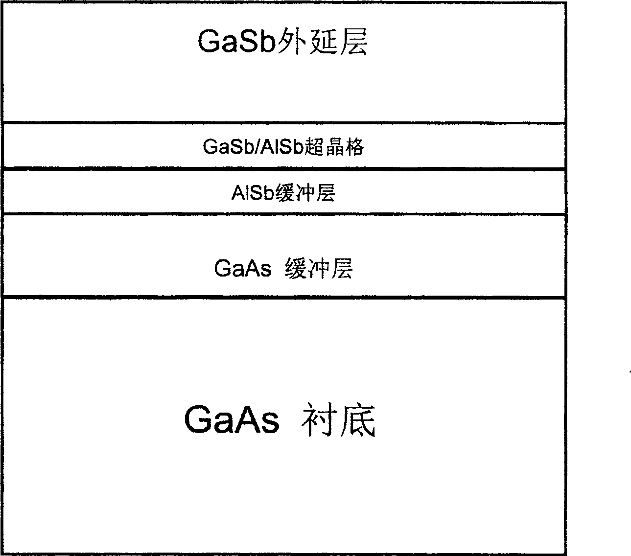
[0069] After deoxidizing and degassing the cleaned GaAs substrate at high temperature, the temperature of the GaAs substrate is lowered to 580°C, the shutter of the Ga source furnace is turned on, and the Ga source temperature is 1150°C, the GaAs high temperature buffer layer is crystallized on the GaAs substrate Grow. The growth time of the GaAs buffer layer is 30 minutes, and the thickness is 0.5 μm. The pressure of the molecular beam epitaxial growth chamber is 5×10 -9 mbar.

[0070] Then close the Ga source furnace shutter, lower the substrate temperature to about 550°C, close the As source furnace shutter, open the Sb source furnace shutter, and open the Al source furnace shutter. The Al source temperature is 1180°C, and a low-temperature AlSb buffer is grown on the GaAs buffer layer. The layer has a growth time of 12 minutes and a thickness of about 100 nm. The pressure of the molecular beam epitaxial growth chamber is 5×10 -9 mbar.

[0071] Then the Al source furnace shutte...

Embodiment 2、3

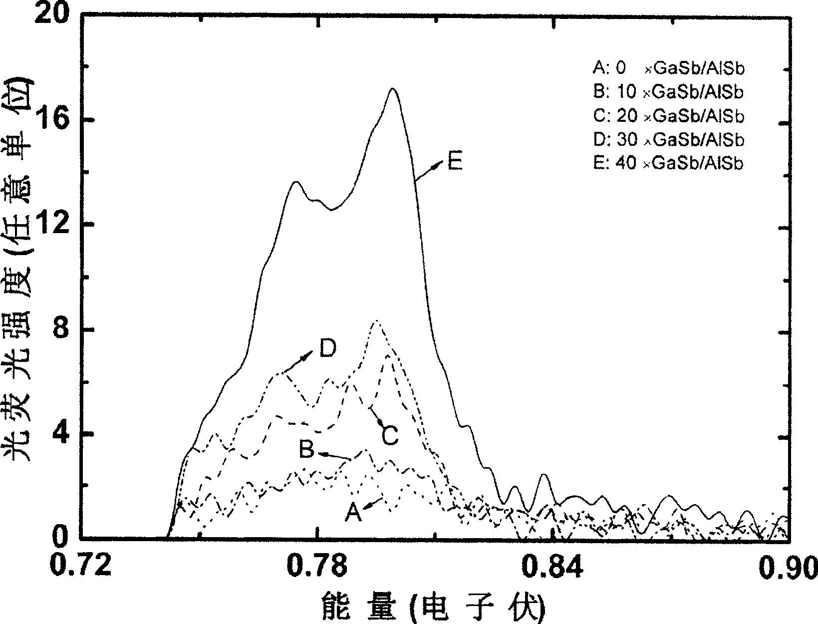
[0074] The GaSb / AlSb superlattices with different periods are 20(C) and 30(D), and the rest are the same as in Example 1. The PL spectrum measured at 10K is as follows image 3 Shown.


PUM


Abstract

The invention discloses a method of the epitaxial growth GaSb on a gallium arsenide substrate. A three buffer layers growth process is adopted in the method. The method specifically comprises the following steps: firstly, a GaAs buffer layer grows on a GaAs substrate under the condition of 580 DEG C; secondly, an AlSb buffer layer grows on the grown GaAs buffer layer under the condition of 550 DEG C; thirdly, a GaSb / AlSb super crystal lattice buffer layer grows on the AlSb buffer layer under the condition of 450 DEG C; fourthly, a GaSb epitaxial layer grows on the GaSb / AlSb super crystal lattice buffer layer under the condition of 400 to 500 DEG C. By utilizing the invention, a doublebuffer layer process is changed into a three-buffer layer process, firstly the GaAs buffer layer grows on the GaAs substrate, then the AlSb buffer layer grows on the grown GaAs buffer layer, the GaSb / AlSb super crystal lattice buffer layer grows on the AlSb buffer layer, finally the GaSb epitaxial layer grows on the GaSb / AlSb super crystal lattice buffer layer, and the perforating dislocation is reduced effectively, thereby the optical quality of the GaSb epitaxial layer is enhanced.

Description

Technical field [0001] The invention relates to a gallium antimonide (GaSb) crystal epitaxial growth technology, in particular to a method for epitaxially growing GaSb on a gallium arsenide (GaAs) substrate by adopting a three-buffer layer growth process. Background technique [0002] GaSb-based semiconductor material (lattice constant of 6.1 InAs, GaSb, AlSb and their ternary compounds), both in terms of optical and electrical properties, they make up for the shortcomings of traditional semiconductor materials. It is the preparation of high-speed, low-power electronic devices-high electron mobility transistors (HEMT ) Or the first choice new materials for mid- and far infrared detectors and lasers (InAs / GaSb, superlattice infrared detectors and lasers). [0003] Although GaSb single wafer has been commercialized, it has disadvantages such as high cost and lack of semi-insulating substrate, so people usually prepare GaSb epitaxial layer on GaAs substrate. In the heteroepitaxial ...

Claims


Application Information

Patent Timeline
Patent Type & Authority Patents(China)
IPC IPC(8): H01L21/203
Inventor 郝瑞亭周志强任正伟徐应强牛智川
Owner INST OF SEMICONDUCTORS - CHINESE ACAD OF SCI
Why Eureka
Try Eureka