

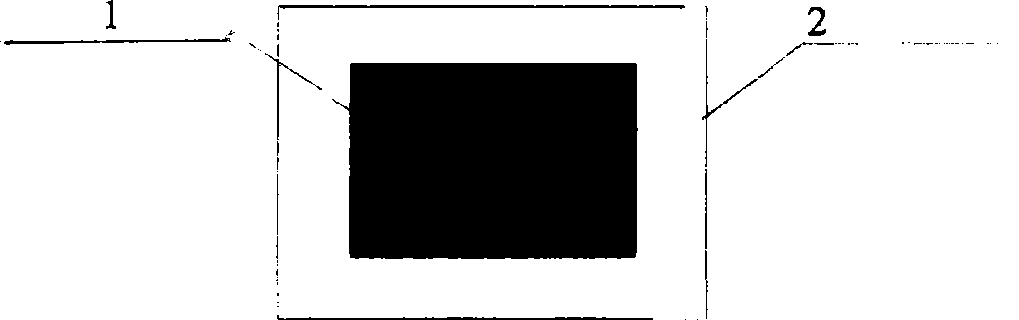
Te-In-Hg photoelectronic detector
A photodetector, indium mercury telluride technology, applied in the field of optoelectronics, can solve the problems of device response speed, unfavorable bandwidth, large junction capacitance, etc., and achieve the effects of avoiding signal loss, reducing junction capacitance, and improving response speed.
- Summary
- Abstract
- Description
- Claims
- Application Information
AI Technical Summary
Problems solved by technology
Method used
Image

Examples
Embodiment 1
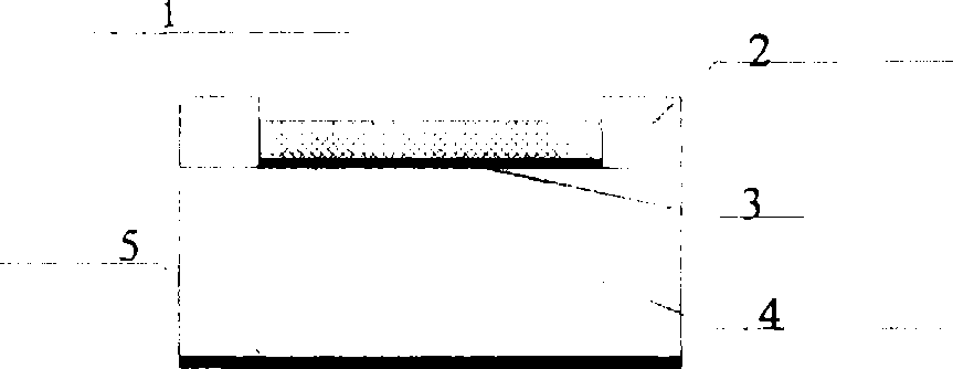
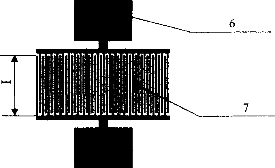
[0031] 1) In the grown Indium Mercury Telluride Intrinsic Oxide Film + SiO 2 On the indium mercury telluride wafer of the passivation protection layer, the oxide film + SiO is removed by using photolithography technology and buffered hydrofluoric acid corrosion 2 The protective layer is passivated to form an interdigitated Schottky junction contact window with a finger width of 10 μm, a finger spacing of 10 μm, and a finger length of 2500 μm.
[0032] 2) A PECVD plasma oxidation method is used to grow a 15nm Indium Mercury Telluride intrinsic oxide layer in the Schottky contact window.
[0033] 3) A 150nm transparent metal electrode (ITO) film is evaporated or sputtered on the surface of the wafer by magnetron sputtering to form a Schottky junction contact with Indium Mercury Telluride.
[0034] 4) Use photolithography technology and lift-off process to remove the ITO film in the area other than the electrodes to form an interdigitated double Schottky junction contact electro...
Embodiment 2
[0037] In the grown oxide layer + SiO 2 On the passivation protective layer on the Indium Mercury Telluride wafer, use photolithography technology and buffered hydrofluoric acid corrosion to remove the Indium Mercury Telluride oxide film + SiO 2 After passivating the protective layer and forming an interdigitated Schottky junction contact window with a finger width of 2 μm, a finger spacing of 10 μm, and a finger length of 1000 μm, the rest of the process steps and parameters are the same as in Example 1.
PUM
 Abstract
Description
Claims
Application Information