A structure and production method of reducing heterogeneous knot dual-crystal tube B-C knotted capacitance

A technology of heterojunction bipolar and manufacturing method, which is applied in semiconductor/solid-state device manufacturing, circuits, electrical components, etc., can solve the problems of the current gain cut-off frequency, the highest oscillation frequency, the increase of the base resistance Rb, etc. The effect of the highest oscillation frequency and strong size controllability

Active Publication Date: 2022-08-05
XIAMEN SANAN INTEGRATED CIRCUIT
View PDF0 Cites 0 Cited by
  • Summary
  • Abstract
  • Description
  • Claims
  • Application Information

AI Technical Summary

Problems solved by technology

The traditional method of reducing the b-c junction capacitance (Cbc) is to directly reduce the base metal width (WB) by photolithography to reduce the BC junction area (Abc) and achieve the effect of reducing the b-c junction capacitance (Cbc); but The reduction of the base metal width (WB) will lead to an increase of the base resistance Rb, which has an adverse effect on the current gain cutoff frequency (ft) and the maximum oscillation frequency (fmax) of the device

Method used


Image

  • A structure and production method of reducing heterogeneous knot dual-crystal tube B-C knotted capacitance
  • A structure and production method of reducing heterogeneous knot dual-crystal tube B-C knotted capacitance
  • A structure and production method of reducing heterogeneous knot dual-crystal tube B-C knotted capacitance

Examples


Embodiment 1

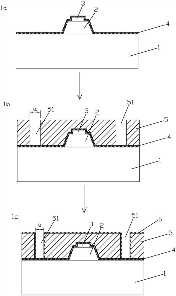
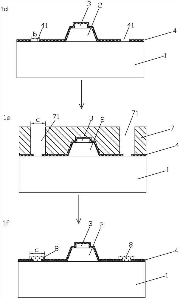
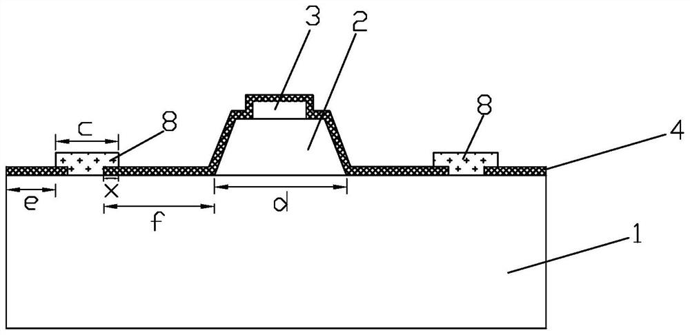
[0029] refer to figure 1 The process flow chart of , taking the formation of a base metal with a bottom line width of about 0.25μm as an example, a manufacturing method for reducing the b-c junction capacitance of a heterojunction bipolar transistor is specifically described:

[0030] First, a chip structure that has been partially fabricated is provided, including an epitaxial layer 1 , an emitter structure (emitter mesa 2 and an emitter metal 3 ) and a passivation layer 4 . The process of the above structure refers to the known process, wherein after the emitter metal 3 is fabricated, a layer of 20-80 nm SiN or SO is deposited by PVCVD 2 As the passivation layer 4, the obtained structure is as figure 1 as shown in a;

[0031] Then, a first photoresist 5 with a thickness of 0.5-1.0 μm is coated on the chip structure, and the first photoresist 5 is a positive photoresist AR80 (from Tokyo Yinghua), which is exposed by an I-line lithography machine. TMAH (concentration 2.38%)...


PUM

PropertyMeasurementUnit
thicknessaaaaaaaaaa
thicknessaaaaaaaaaa

Abstract

The present invention disclosed a structure and production method of reducing heterogeneous knot double -pole transistors B‑c knot capacitance. When making the base metal, first painting the first light barrier on the chip structureThe window, then coat the second light barrier, reduce the line width of the first window through the slightly shrinking and backflow process, etch the passivation layer in the first window to form the first opening, remove the third light obstruction and expose after removing the light resistance, and expose it.The second window formed on the first opening, and the line width of the second window is larger than that of the first opening, and then the deposit fund belongs to the second window and the base metal is formed in the first opening to remove the light resistance.The present invention has formed a base metal structure with width less than the top line. Without increasing the base resistance, the B -C edging area is reduced to reduce the effect of reducing the BAC connection capacitance, thereby improving the maximum oscillationfrequency.

Description

technical field [0001] The invention relates to the technical field of semiconductors, and in particular, to a structure and a manufacturing method for reducing the b-c junction capacitance of a heterojunction bipolar transistor. Background technique [0002] With the development of HBT technology, higher requirements are put forward for high frequency parameters. There are two main high-frequency parameters, one is the current gain cut-off frequency (ft); the other is the highest oscillation frequency (fmax). The maximum oscillation frequency (fmax) is inversely proportional to the product of the base resistance (Rb) and the b-c junction capacitance (Cbc), so in order to increase the maximum oscillation frequency (fmax), the b-c junction capacitance (Cbc) and base resistance (Rb) must be reduced ). The traditional method of reducing the b-c junction capacitance (Cbc) is to directly reduce the base metal width (WB) by photolithography to reduce the BC junction area (Abc) a...

Claims


Application Information

Patent Timeline
Patent Type & Authority Patents(China)
IPC IPC(8): H01L21/331H01L21/28H01L29/423H01L29/737
CPCH01L29/66242H01L21/28H01L29/737H01L29/42304
Inventor 何湘阳郭佳衢魏鸿基
Owner XIAMEN SANAN INTEGRATED CIRCUIT
Why Eureka
Try Eureka