Preparation method for preparing gallium nitride schottky diode

A gallium nitride Schottky and diode technology, applied in semiconductor/solid-state device manufacturing, semiconductor devices, electrical components, etc., to achieve the effect of improving lifespan and reducing Schottky contact resistance

Active Publication Date: 2017-08-29
PEKING UNIV +1
View PDF3 Cites 0 Cited by
  • Summary
  • Abstract
  • Description
  • Claims
  • Application Information

AI Technical Summary

Problems solved by technology

[0004] The invention provides a method for preparing gallium nitride Schottky diodes, which is used to solve the problem that the Schottky contact resistance generated during the preparation process of the existing gallium nitride Schottky diodes will be much greater than the ohmic contact resistance , to achieve the beneficial effects of reducing Schottky contact resistance and improving the life of GaN Schottky diodes

Method used


Image

  • Preparation method for preparing gallium nitride schottky diode
  • Preparation method for preparing gallium nitride schottky diode
  • Preparation method for preparing gallium nitride schottky diode

Examples


Embodiment Construction

[0042] In order to make the purpose, technical solutions and advantages of the embodiments of the present invention clearer, the technical solutions in the embodiments of the present invention will be clearly and completely described below in conjunction with the drawings in the embodiments of the present invention. Obviously, the described embodiments It is a part of embodiments of the present invention, but not all embodiments. Based on the embodiments of the present invention, all other embodiments obtained by persons of ordinary skill in the art without making creative efforts belong to the protection scope of the present invention.

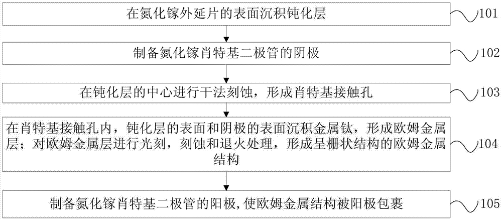
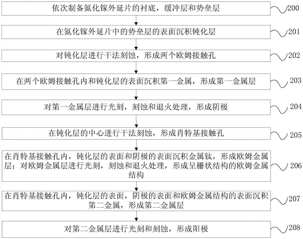
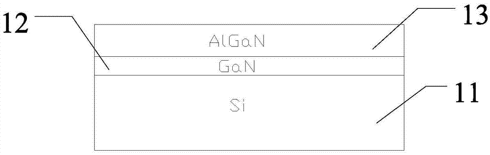
[0043] figure 1 A schematic flow chart of a method for preparing a gallium nitride Schottky diode provided in Embodiment 1 of the present invention, as shown in figure 1 Shown preparation method comprises the steps:

[0044] Step 101, depositing a passivation layer on the surface of the gallium nitride epitaxial wafer.

[0045] Step 102, p...


PUM

PropertyMeasurementUnit
thicknessaaaaaaaaaa

Abstract

The invention provides a preparation method for preparing a gallium nitride schottky diode. According to the method, a passivation layer is deposited on the surface of a gallium nitride epitaxial wafer, and the cathode of a gallium nitride schottky diode is prepared. The center of the passivation layer is subjected to the dry etching process, so that a schottky contact hole is formed. In the schottky contact hole, the metal titanium is deposited on the surface of the passivation layer and the surface of the cathode, so that an ohmic metal layer is formed. The ohmic metal layer is subjected to lithography, etching and annealing, and then an ohmic metal structure of a grid-shaped structure is formed. The anode of the gallium nitride schottky diode is prepared. The ohmic metal structure is in the shape of a grid-shaped structure, and is wrapped by the anode. As a result, on the premise that the output performance of the gallium nitride schottky diode is not influenced at all, the area of a schottky junction is reduced. Therefore, the schottky contact resistance is reduced. Meanwhile, the device performance of the gallium nitride schottky diode is improved, and the lifetime of the gallium nitride schottky diode is prolonged.

Description

technical field [0001] The invention relates to the technical field of semiconductors, in particular to a method for preparing a gallium nitride Schottky diode. Background technique [0002] A Schottky diode is a semiconductor device made using a metal contact semiconductor layer. Compared with semiconductor diodes in the traditional sense, it has the characteristics of extremely short reverse recovery time. Therefore, Schottky diodes are widely used in switching power supplies, frequency converters, drives and other circuits. Gallium nitride material is the third generation wide bandgap semiconductor material. Because of its large bandgap width, high electron saturation rate, high breakdown electric field, high thermal conductivity, corrosion resistance and radiation resistance, it has become the ideal choice for the preparation of short-wavelength optoelectronics. The best material for devices and high-voltage high-frequency high-power devices. To sum up, the Schottky di...

Claims


Application Information

Patent Timeline
Patent Type & Authority Applications(China)
IPC IPC(8): H01L21/329H01L29/872
CPCH01L29/66143H01L29/872H01L2229/00
Inventor 刘美华孙辉林信南陈建国
Owner PEKING UNIV
Why Eureka
Try Eureka