Lateral SOI high voltage device with instantaneous dose rate radiation hardened structure
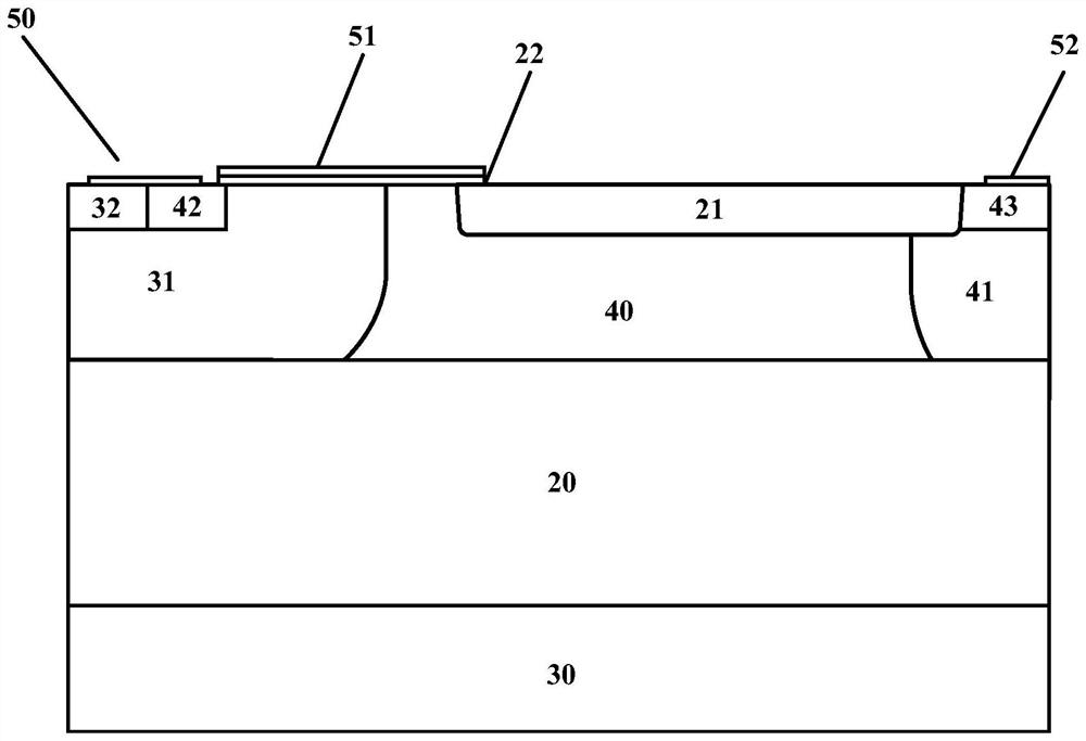
A radiation-hardened, high-voltage device technology, applied in the direction of semiconductor devices, electrical components, circuits, etc., can solve the problems of wrong signal output, parasitic device opening, device burnout, etc., and achieve good compatibility, reduce strength, and reduce the number of effects
- Summary
- Abstract
- Description
- Claims
- Application Information
AI Technical Summary
Problems solved by technology
Method used
Image
Examples
Embodiment 1
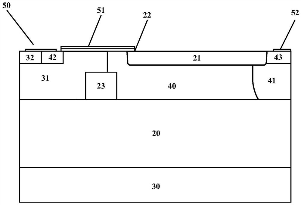
[0029] Such as figure 2 As shown, a lateral SOI high-voltage device with an instantaneous dose rate radiation-hardened structure in this embodiment includes a second-type impurity-doped semiconductor substrate 30; formed on the second-type impurity-doped semiconductor substrate 30 The buried oxide layer 20; the first type doped impurity drift region 40 and the second type doped impurity well region 31 formed on the buried oxide layer 20; the second type doped impurity well region 31 formed on the second type doped impurity well region The second type doped impurity contact region 32 and the first type doped impurity source region 42; the first type doped impurity well region 41 formed on the right side of the first type doped impurity drift region 40; The first type doped impurity drain region 43 formed in the first type doped impurity well region 41; the first type doped impurity drift region 40 formed at the junction of the second type doped impurity well region 31 The ins...
Embodiment 2
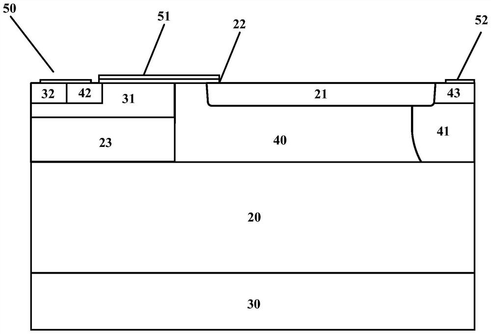
[0037] Such as image 3 As shown, the difference between this embodiment and Embodiment 1 is: the lower end surface of the insulating dielectric buried layer 23 is connected to the buried oxide layer 20, the insulating dielectric buried layer 23 intersects with the left edge of the second-type doped impurity well region 31, and the insulating The right side of the dielectric buried layer 23 intersects the right edge of the second type doped impurity well region 31 . This effectively reduces the area where electron-hole pairs are generated after the device is irradiated with the instantaneous dose rate, that is, the number of electron-hole pairs generated after the device is irradiated with the instantaneous dose rate is reduced, and the photocurrent is reduced.
Embodiment 3
[0039] Such as Figure 4As shown, the difference between this embodiment and Embodiment 1 is that the lower end surface of the insulating dielectric buried layer 23 is not connected to the buried oxide layer 20 . This also effectively reduces the area where electron-hole pairs are generated after the device is irradiated with the instantaneous dose rate, that is, the number of electron-hole pairs generated after the device is irradiated with the instantaneous dose rate is reduced, and the photocurrent is reduced.
PUM
 Abstract
Description
Claims
Application Information


