Charged particle beam application device

A technology of charged particles and electrodes, applied in the field of high-speed and high-precision charged particle beam application devices, can solve the problems of difficult voltage correction, large mechanical error of contact resistance, slow response, etc., and achieve the effect of improving the accuracy of irradiation position

Active Publication Date: 2009-09-30
HITACHI HIGH-TECH CORP +1
View PDF2 Cites 0 Cited by
  • Summary
  • Abstract
  • Description
  • Claims
  • Application Information

AI Technical Summary

Problems solved by technology

However, since the high-precision surface potentiometer responds slower than the change in the drawing of the electron beam current, it is difficult to calculate the correction voltage at high speed.
That is, the high-speed correction of dynamically correcting the wafer potential during drawing cannot be realized by the surface potentiometer
[0016] Such as in the special publication No. 11-111599 Figure 4 As shown, even if one of the two ground leads in contact with the chip is used for potential measurement, and the power supply for correction is connected to the other, although the surface potential of the chip can be corrected in principle, this method uses two ground leads. The premise is that the resistance of the leads is low. On the other hand, the mechanical error of the contact resistance between the ground lead and the chip is extremely large, and the reproducibility cannot be guaranteed. Therefore, it is difficult to correct the potential of the chip frequently and accurately by this method.

Method used


Image

  • Charged particle beam application device
  • Charged particle beam application device
  • Charged particle beam application device

Examples


Embodiment 1

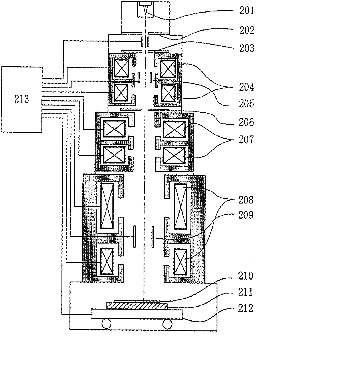
[0059] figure 2 A schematic diagram of the overall structure of the electron beam wafer drawing apparatus is shown in . The electron beam emitted from the thermionic source 201 is accelerated toward the anode electrode 202 and directly irradiates the first mask 203 . A single rectangular opening is provided on the first mask, and an image of the opening is obtained by irradiating electron beams. An aperture image of the first mask is formed on the second mask 206 by the forming lens 204 . The second mask is provided with a rectangular opening for the variable shaping irradiation method and a shaping opening for the collective pattern irradiation method. The shape and area of ​​the electron beam are determined by controlling the imaging position on the second mask by the deflector 205 for electron beam shaping. The electron beams passing through the openings of the second mask are projected onto a wafer 210 as a sample by a reduction lens 207 and an objective lens 208 . A ...

Embodiment 2

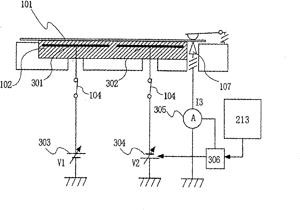
[0069] In Example 1, a DC power supply was connected to both sides of the bipolar electrodes, and a closed circuit was formed between the two electrodes to reduce the value of the current flowing from the adsorption electrodes to the wafer. However, in reality, in addition to the leakage current from the adsorption electrode, there is also the current of the irradiated electron beam in the wafer. Most of this electron beam flows into ground potential via the ground lead. This is because, unlike the resistance between the wafer and the adsorption electrode, which can be kept high by means of a dielectric, the contact resistance between the wafer and the ground lead is much lower.

[0070] Therefore, by using the method of Example 1 before drawing, even if the sum of the leakage currents flowing from the adsorption electrodes to the wafer is reduced, once the electron beam current irradiation starts, a potential difference is generated between the wafer and the ground potential....

Embodiment 3

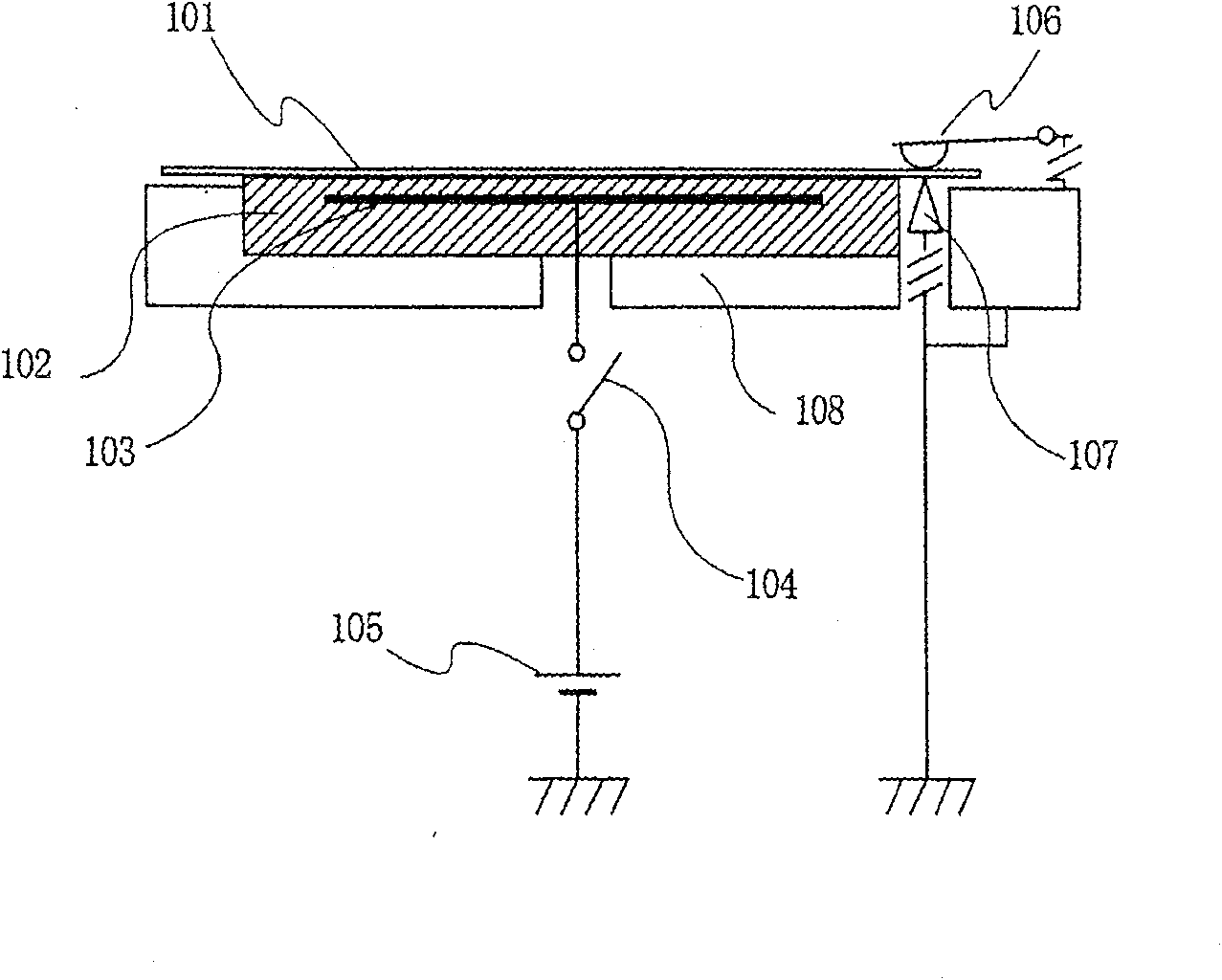
[0088] use Figure 6 The schematic diagrams in the figure illustrate the electrostatic adsorption device of this embodiment. In addition, the electrostatic adsorption device of this embodiment is also the same as that of Embodiment 1, assuming that it is installed in figure 2 The electron beam profiling setup shown.

[0089] This embodiment is an embodiment using a plurality of ground leads. The DC power supply 105 is connected to the adsorption electrode 103 buried in the dielectric 102 through the switch 104, and is given a potential difference V1 from the ground potential. In this embodiment two ground leads 601 and 602 are pressed on the backside of the chip 101 . Power sources 605 and 606 for wafer potential correction are connected to the ground leads via ammeters 603 and 604, respectively. Wafer potential correction power supplies 605 and 606 apply DC potential differences V3 and V4 between the ground potential and the ground lead, respectively, and ammeters 603 an...


PUM


Abstract

Provided is a charged particle beam application device. The potential of the wafer is dynamically detected during drawing, and the potential is corrected to improve the positional accuracy of the circuit pattern drawn on the wafer. After measuring the contact resistance formed by the wafer (101, sample) and the ground lead (107, contact terminal), measure the current flowing from the wafer (101, sample) to the ground potential via the ground lead (107, contact terminal), according to As a result of the measurement, a potential difference is applied between the wafer (101, sample) and the ground potential.

Description

technical field [0001] The present invention relates to a semiconductor manufacturing device and a semiconductor inspection device used in a semiconductor process, and more particularly to a high-speed and high-precision charged particle beam application device. Background technique [0002] One of the main steps of forming an LSI pattern on a semiconductor substrate is electron beam drawing, which forms a circuit pattern by irradiating electron beams on a wafer coated with a photosensitive material. In this electron beam drawing device, an electrostatic adsorption device is used for holding and straightening a wafer in a vacuum. [0003] figure 1 A cross-sectional view of a typical electrostatic adsorption electrode used in a conventional electron beam mapping device is shown in . 101 is a semiconductor wafer as a sample (hereinafter referred to as a wafer), 102 is a dielectric made of alumina as a main material, and 103 is an adsorption electrode embedded in the dielectr...

Claims


Application Information

Patent Timeline
Patent Type & Authority Patents(China)
IPC IPC(8): H01L21/00H01L21/68H05H1/46H01J37/00
Inventor 谷本明佳早田康成菅谷昌和远山博堤刚志染田恭宏
Owner HITACHI HIGH-TECH CORP
Why Eureka
Try Eureka