
Thin membrane encapsulation structure of fingerprint identifying device

A technology of fingerprint identification and thin-film packaging, which is applied in the field of thin-film packaging structure of fingerprint readers, which can solve the problems of no products, overflowing glue, and the inability to continue to use packaging processes and equipment, etc.

Inactive Publication Date: 2009-10-07
CHIPMOS TECH INC
View PDF4 Cites 0 Cited by
  • Summary
  • Abstract
  • Description
  • Claims
  • Application Information

AI Technical Summary

Problems solved by technology

The technical method is to first seal the glue and then press a soft board on one side of the chip, which will have the disadvantage of overflowing glue and polluting the sensing area, and cannot continue to use the existing tape-and-reel packaging process and equipment.
[0005] It can be seen that the above-mentioned existing fingerprint reader packaging structure obviously still has inconvenience and defects in structure and use, and needs to be further improved urgently.
In order to solve the problems of the packaging structure of the fingerprint reader, the relevant manufacturers have tried their best to find a solution, but no suitable design has been developed for a long time, and there is no suitable structure for general products to solve the above problems , this is obviously a problem that relevant industry players are eager to solve

Method used


Image

  • Thin membrane encapsulation structure of fingerprint identifying device
  • Thin membrane encapsulation structure of fingerprint identifying device
  • Thin membrane encapsulation structure of fingerprint identifying device

Examples


Embodiment Construction

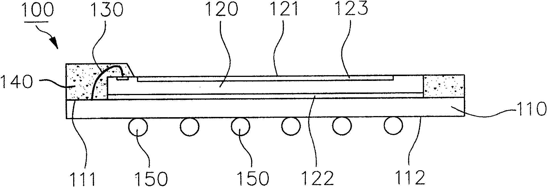
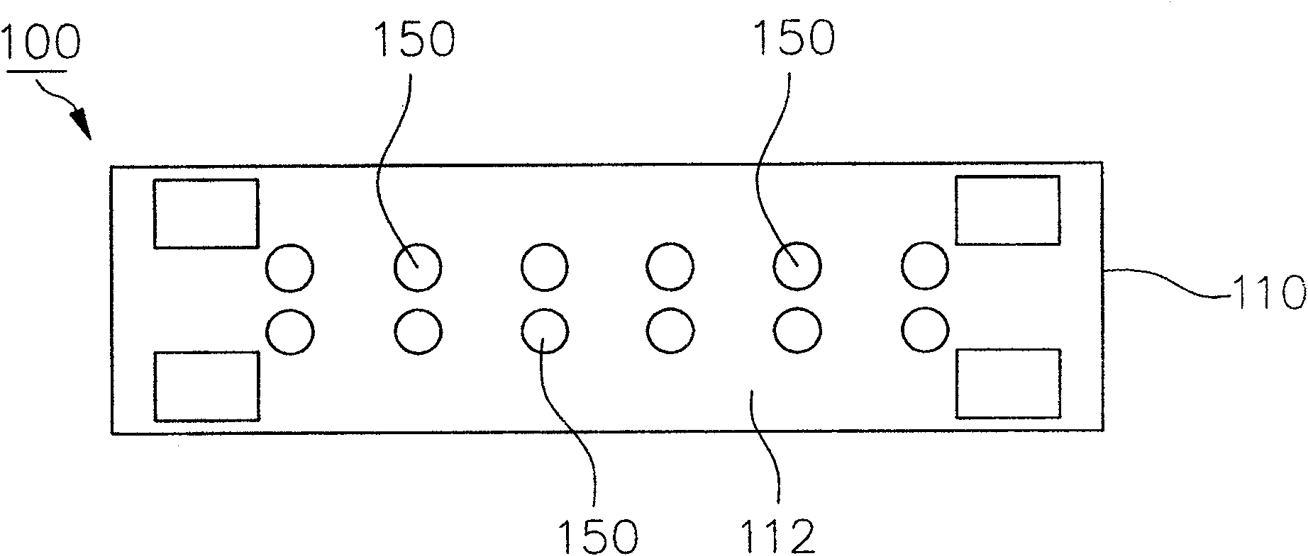
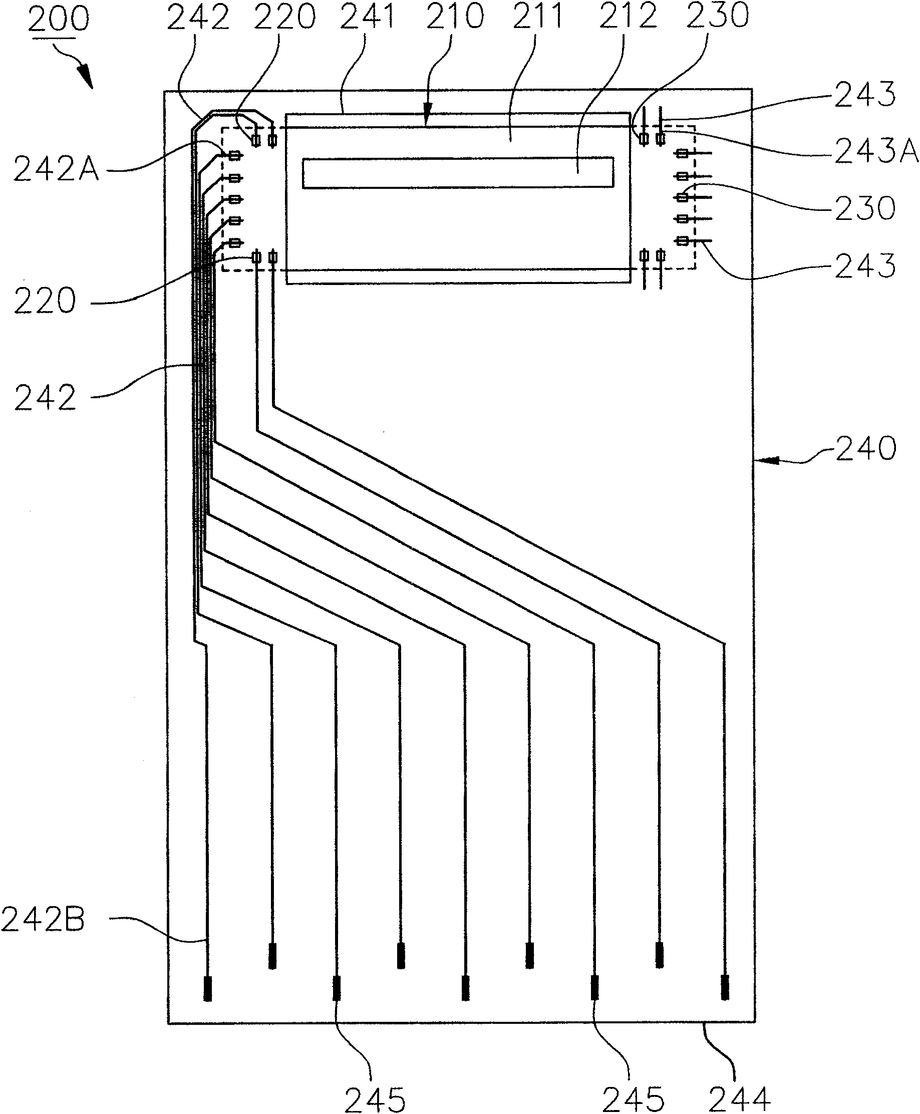
[0055] In order to further explain the technical means and effects that the present invention adopts to achieve the intended purpose of the invention, the specific implementation, structure and characteristics of the film packaging structure of the fingerprint reader proposed according to the present invention will be described below in conjunction with the accompanying drawings and preferred embodiments. And its effect, detailed description is as follows.

[0056] The first physical embodiment of the present invention discloses a film packaging structure of a fingerprint reader. image 3 is a top schematic view of the thin film package structure of the fingerprint reader. Figure 4 It is a schematic diagram of the partial top surface of the thin film packaging structure of the fingerprint reader at the dummy pins. Figure 5 is a schematic cross-sectional view of the film packaging structure of the fingerprint reader.

[0057] see image 3 , Figure 4 and Figure 5 , the ...


PUM


Abstract

The invention relates to a thin film enclosing structure of a fingerprint identifier, comprising a fingerprint identifier chip, a plurality of projecting blocks, a plurality of virtual projecting blocks, a circuit film and sealing colloids. A sensing area is formed on an active surface of the fingerprint identifier chip. The above projecting blocks are arranged on the active surface and are located at one lateral end of the sensing area, and the above virtual projecting blocks are also arranged on the active surface and are located at the opposite lateral end of the sensing area. The circuit film is equipped with a through opening to expose the sensing area and includes a plurality of pins and virtual pins to respectively join the above projecting blocks and virtual projecting blocks, wherein all the outer ends of the pins are confluent at the same side of the circuit film. The sealing colloids are used to seal the above projecting blocks and virtual projecting blocks, thereby reaching the balance of thermo-compression bonding and engagement and facilitating to form the sealing colloids.

Description

technical field [0001] The present invention relates to a fingerprint sensor package, in particular to a thin film packaging structure of a fingerprint sensor. Background technique [0002] The packaging structure of the fingerprint reader can be additionally installed in various electronic products, such as mobile phones, notebook computers, personal digital assistants (PDA, or palmtop computers), etc., to identify users' fingerprints. At present, the fingerprint reader can be manufactured and packaged by using semiconductor manufacturing process. Different from the traditional IC package, the fingerprint reader chip should have an exposed sensing area to be able to identify fingerprints. However, the traditional packaging structure of fingerprint readers uses the traditional substrate and mold packaging technology. The interfaces for mechanical fixing and electrical connection are all located on the bottom surface of the substrate, which makes it difficult to control the h...

Claims


Application Information

Patent Timeline
Patent Type & Authority Patents(China)
IPC IPC(8): H01L23/488H01L23/498G06K9/00
CPCH01L2924/15311H01L2924/0002H01L2924/1815H01L2224/73265H01L24/50H01L2224/48227H01L2224/32225H01L2224/50H01L2924/00H01L2924/00012
Inventor 黄铭亮李耀荣李明勋
Owner CHIPMOS TECH INC
Learn More