High speed signal level switching circuit

A technology for converting circuits and high-speed signals, which is applied in electrical components, impedance networks, single-ended pair networks, etc. It can solve problems such as poor signal quality and impedance mismatch, achieve impedance matching, realize level conversion, and save PCB wiring effect of space

Inactive Publication Date: 2009-10-07
STATE GRID TIANJIN ELECTRIC POWER
View PDF4 Cites 0 Cited by
  • Summary
  • Abstract
  • Description
  • Claims
  • Application Information

AI Technical Summary

Problems solved by technology

[0009] In view of the above problems, the object of the present invention is to provide a high-speed level conversion circuit, which overcomes the disadvantages of the cost and PCB area of ​​the method 1 in the prior art, and the poor signal quality caused by the impedance mismatch in the method 2 The problem

Method used


Image

  • High speed signal level switching circuit
  • High speed signal level switching circuit
  • High speed signal level switching circuit

Examples


Embodiment Construction

[0026] The preferred embodiments of the present invention will be described below in conjunction with the accompanying drawings. It should be understood that the preferred embodiments described here are only used to illustrate and explain the present invention, and are not intended to limit the present invention.

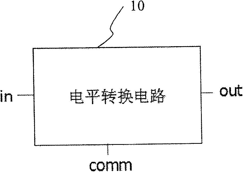
[0027] figure 1 It is a terminal schematic diagram of a high-speed level conversion circuit of an embodiment of the present invention. Such as figure 1 As shown, the level conversion circuit 10 of the present invention has three terminals, namely in, out, and comm.

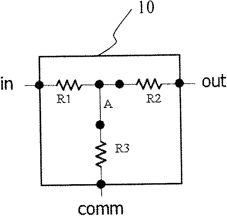
[0028] figure 2 It is a structural schematic diagram of the level conversion circuit of the present invention. Such as figure 2 As shown, the high-speed level conversion circuit 10 includes resistors R1, R2, and R3 for converting a signal of a high power supply voltage into a signal of a low power supply voltage and performing impedance matching between a signal of a high power supply voltage an...


PUM


Abstract

The invention discloses a high-speed signal level conversion circuit. The high-speed signal level conversion circuit includes a first terminal, one end of which is used to connect a signal with a first power supply voltage, and the other end is connected to a first resistor; a second terminal, one end of which is used to connect a The signal of the second power supply voltage, the other end is connected to the second resistor; the third terminal is used to connect the reference voltage of the high-speed level conversion circuit at one end, and the other end is connected to the third resistor; wherein, the first resistor, the second resistor The two resistors and the third resistor are connected to form a T-shaped network, which is used to convert the signal of the first source voltage into the signal of the second power supply, and convert the signal of the first source voltage to the signal of the second power supply Voltage signals are impedance matched.

Description

technical field [0001] The invention relates to a high-speed signal level conversion circuit, in particular to the level conversion of high-speed signals in the fields of communication and IT. Background technique [0002] The level conversion of high-speed signals commonly used in the communication and IT fields is usually implemented in two ways, namely, the first way: using an IC chip for level conversion; the second way: using a circuit of two resistor voltage dividers. [0003] Figure 4 and Figure 5 Schematic diagrams of level shifting in the prior art using the first method and the second method are respectively shown. [0004] Such as Figure 4 As shown, in mode one, the level of the driving device 42 of the 5V power supply is converted to 3.3V by the IC chip 44 for level shifting, and then output to the receiving device 46 of the 3.3V power supply. [0005] For the first method of IC chips using level shifting, the cost is high, and the area occupied by the PCB i...

Claims


Application Information

Patent Timeline
Patent Type & Authority Patents(China)
IPC IPC(8): H03H5/12
Inventor 眭诗菊张加民
Owner STATE GRID TIANJIN ELECTRIC POWER
Why Eureka
Try Eureka