Packaging substrate structure with electronic component embedded therein and method for manufacture of the same

a technology of electronic components and packaging substrates, applied in the incorporation of printed electric components, printed circuit aspects, non-metallic protective coating applications, etc., can solve the problems of poor electrical performance, inability to meet the demands of compact and lightweight electronic devices, and inability to achieve the purpose of miniaturization, etc., to save the space for wiring layout and enhance electrical performance.

Active Publication Date: 2009-03-05
UNIMICRON TECH CORP
View PDF7 Cites 14 Cited by
  • Summary
  • Abstract
  • Description
  • Claims
  • Application Information

AI Technical Summary

Benefits of technology

[0008]The object of the present invention is to provide a packaging substrate structure with an electronic component embedded therein and a method for manufacturing the same so as to save the space for wiring layout and to enhance electrical performance.

Problems solved by technology

Accordingly, the purpose for miniaturization cannot be achieved.
In addition, the number of the passive components 14 is limited to the restricted area of the packaging substrate 10, and thereby the demands for compact and lightweight electronic devices have not been met.
Furthermore, the fact that passive components 14 are disposed on the surface of the packaging substrate 13 causes long transmission paths, large parasitic induction, poor electrical performance and thus the accuracy of signal transmission is badly influenced.
Besides, the passive components 14 disposed on the surface of the packaging substrate 13 make the height of the package structure increase and thus the demand for a light and compact-sized product cannot be met.

Method used


Image

  • Packaging substrate structure with electronic component embedded therein and method for manufacture of the same
  • Packaging substrate structure with electronic component embedded therein and method for manufacture of the same
  • Packaging substrate structure with electronic component embedded therein and method for manufacture of the same

Examples


embodiment 1

Structure Embodiment 1

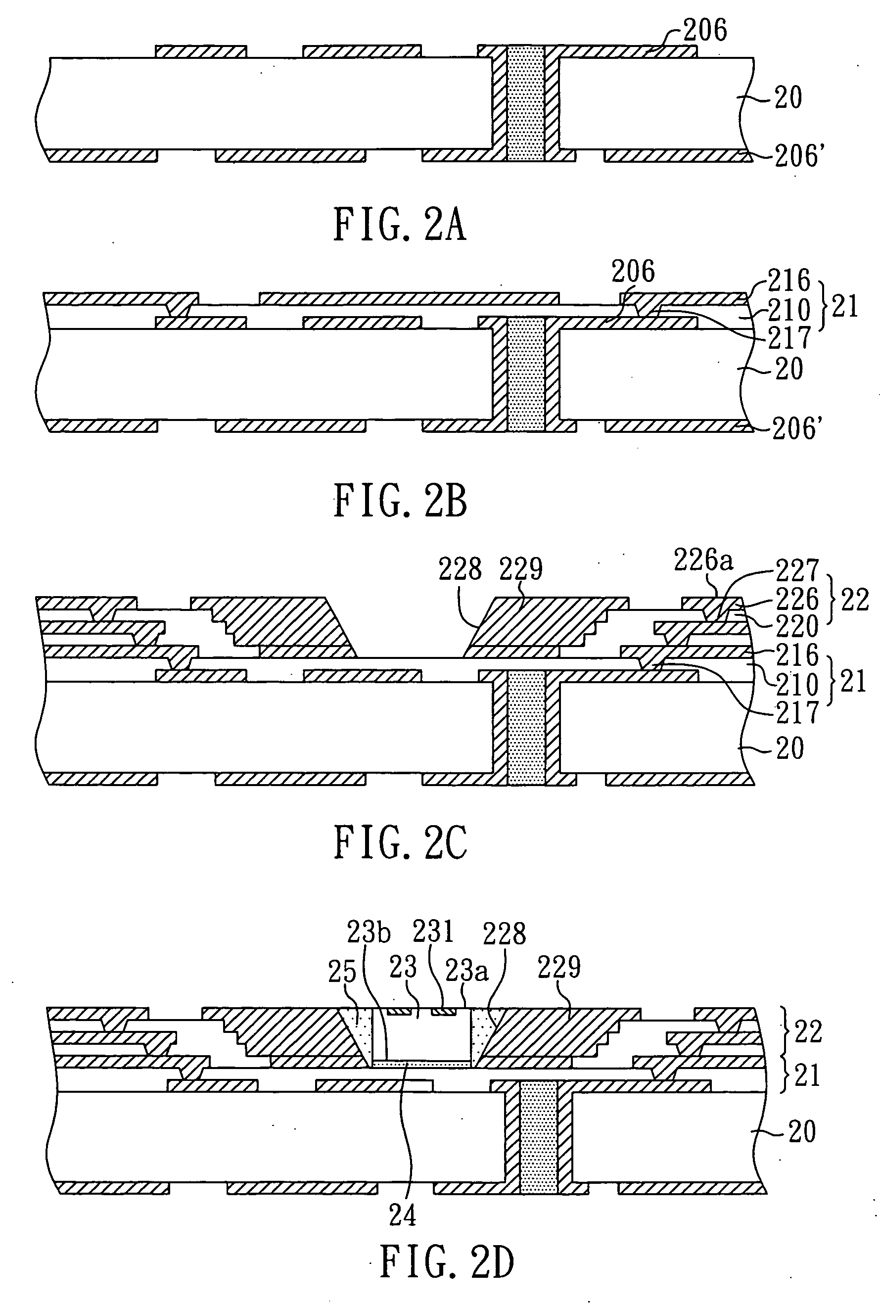
[0037]With reference to FIGS. 2E and 2F, the packaging substrate structure with an electronic component embedded therein according to the present embodiment comprises: a core board 20; a first built-up structure 21, 21′ disposed on at least one surface of the core board 20 and comprising at least one first dielectric layer 210, at least one first wiring layer 216 disposed on the first dielectric layer 210, and a plurality of first conductive vias 217; a second built-up structure 22, 22′ disposed on the surface of the first built-up structure 21, 21′ and having a cavity 228 to expose the first built-up structure 21, 21′; an electronic component 23 disposed in the cavity 228 and having an active surface 23a and an inactive surface 23b, wherein the active surface 23a has a plurality of electrode pads 231, and the inactive surface 23b faces the first built-up structure 21; and a solder mask 27 disposed on the surfaces of the second built-up structure 22, 22′ and th...

embodiment 2

Method and Structure Embodiment 2

[0043]The method and the structure in the present embodiment are the same as those in Method Embodiment 1 and Structure Embodiment 1, except the outmost wiring layer 216 of the first built-up structure has a metal layer 219 corresponding to the cavity 228 of the second built-up structure 22 for attaching the inactive surface 22b of the electronic component 22 as shown in FIG. 4.

embodiment 3

Method and Structure Embodiment 3

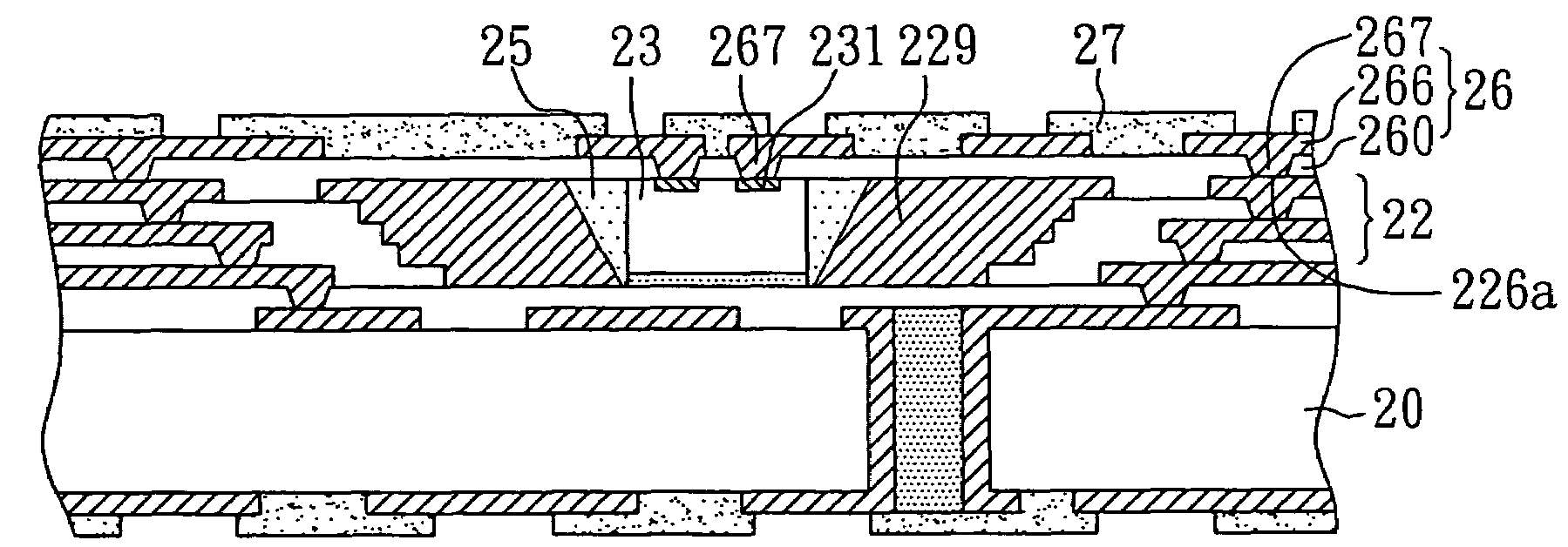
[0044]The method and the structure in the present embodiment are the same as those in Method Embodiment 1 and Structure Embodiment 1, except a third built-up structure 26 can further be formed between the solder mask 27 and the second built-up structure 22 together with the electronic component 23 as shown in FIG. 5. Herein, the third built-up structure 26 has at least one third dielectric layer 260, at least one third wiring layer 266 disposed on the third dielectric layer 260, and a plurality of third conductive vias 267. In addition, a part of the third conductive vias 267 in the third built-up structure 25 electrically connect to the conductive pads 226a of the second built-up structure 22, and another part of the third conductive vias 267 electrically connect to the electrode pads 231 of the electronic component 23.

[0045]Although the present invention only illustrates the structure where the built-up structure is formed on only one side of the c...


PUM


Abstract

A packaging substrate structure with an electronic component embedded therein and a fabricating method thereof are disclosed. The packaging substrate structure comprises a core plate; a first built-up structure disposed on a surface of the core plate and comprising a first dielectric layer and a first circuit layer disposed on the first dielectric layer; a second built-up structure disposed on the first built-up structure, wherein a cavity is disposed in the second built-up structure to expose the first built-up structure; an electronic component disposed in the cavity, wherein the electronic component has an active surface having a plurality of electrode pads and an inactive surface facing the first built-up structure; and a solder mask disposed on the surfaces of the second built-up structure and the electronic component, and having a plurality of first openings to expose the electrode pads of the electronic component.

Description

BACKGROUND OF THE INVENTION[0001]1. Field of the Invention[0002]The present invention relates to a packaging substrate structure with an electronic component embedded therein and a method for manufacturing the same and, more particularly, to a packaging substrate structure, which exhibits enhanced electrical performance and reduces costs, with electronic components embedded therein and a method for manufacturing the same.[0003]2. Description of Related Art[0004]As the electronic industry develops rapidly, the technology of semiconductor packaging accordingly moves towards integration and miniaturization so that the demands such as multifunction and high efficiency in electronic devices can be met. In addition, packaging substrates with many active and passive components and circuit connections thereon have advanced from being single-layered boards to multiple-layered boards to expand the space for wiring layout in a limited packaging substrate and to meet the demand of the applicati...

Claims


Application Information

Patent Timeline
Patent Type & Authority Applications(United States)
IPC IPC(8): H01L23/485H01L21/58
CPCH01L23/5389H01L2224/32225H01L24/82H01L2224/2402H01L2224/24227H01L2224/73267H01L2224/92244H01L2924/14H01L2924/15157H01L2924/19041H01L2924/30105H05K1/114H05K1/185H05K3/06H05K3/28H05K2201/09563H05K2201/09845H05K2201/10674H01L2924/01033H01L2224/16225H01L24/24H01L24/05H01L2224/02379H01L2224/05001H01L2224/05024H01L2224/05026H01L2224/05548H01L2224/05571
Inventor HSU, SHIH-PING
Owner UNIMICRON TECH CORP
Why Eureka
Try Eureka