Image sensor module package structure with supporting element

a technology of image sensor and package structure, which is applied in the direction of semiconductor devices, semiconductor/solid-state device details, radiation control devices, etc., can solve the problems of reducing the volume of the image sensor module package structure, affecting affecting the image-sensing sensitivity and the production yield of the resultant light-sensing elements, etc., to achieve enhanced image-sensing sensitivity of the image sensor modul

Active Publication Date: 2009-10-06
KT IMAGING USA LLC
View PDF3 Cites 13 Cited by
  • Summary
  • Abstract
  • Description
  • Claims
  • Application Information

AI Technical Summary

Benefits of technology

[0020]1. A volume of the image sensor module package structure can be reduced;
[0021]2. An image-sensing accuracy and an image-sensing sensitivity of the image sensor module package structure can be enhanced; and
[0022]3. A production yield of the image sensor module package structure can be improved.

Problems solved by technology

Since it is difficult to ensure the absolute clearness of the transparent layer before it is put on the top surface of the base, any defect or stain on the transparent layer can jeopardize the image-sensing sensitivity and the production yield of the resultant light-sensing elements.
On the other hand, in an alternative case, when a light-pervious glass is implemented as the transparent layer, edges thereof tend to be cracked or jagged in a cutting process and thus the production yield of the resultant light-sensing elements is suffered.
Consequently, a wiring space cannot be saved on the conventional image sensor module package structure and thus the image sensor module package structure cannot be further downsized.

Method used


Image

  • Image sensor module package structure with supporting element
  • Image sensor module package structure with supporting element
  • Image sensor module package structure with supporting element

Examples


Embodiment Construction

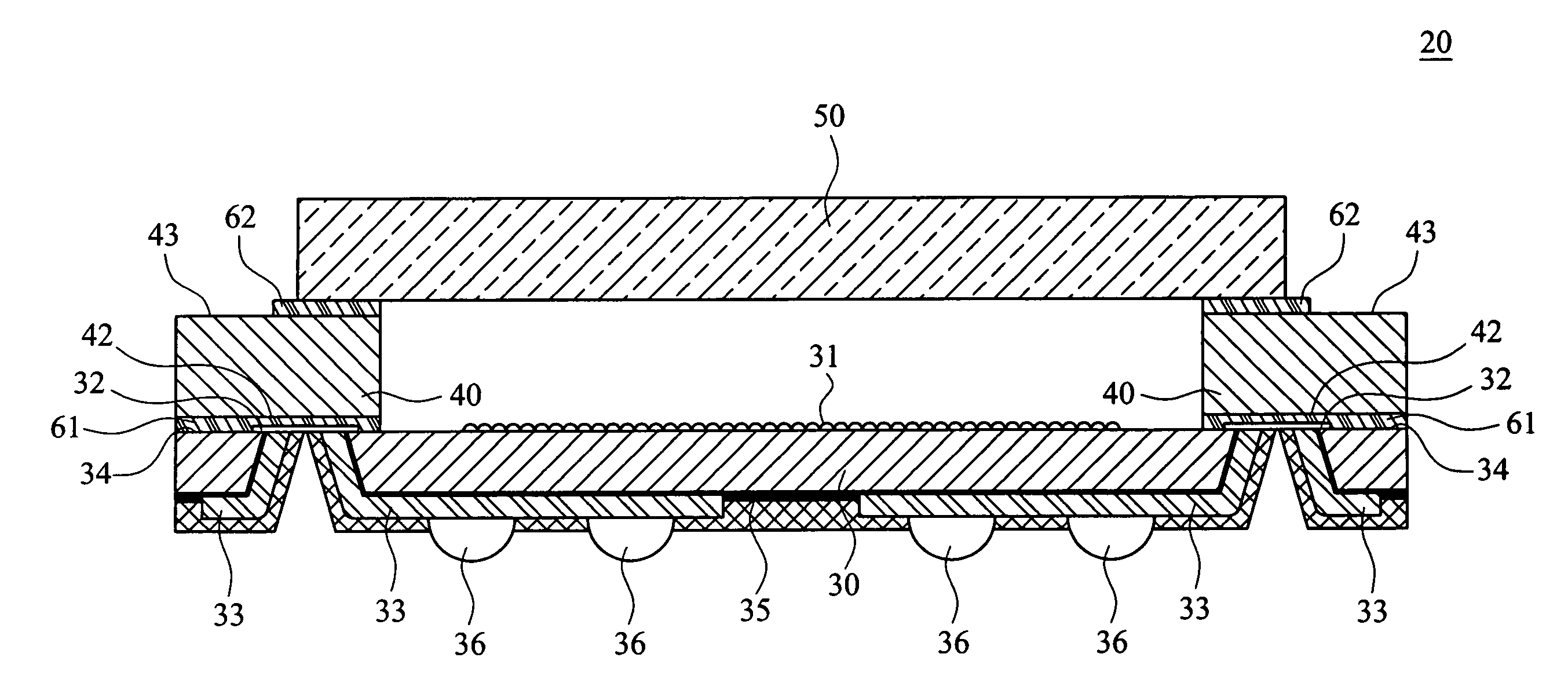
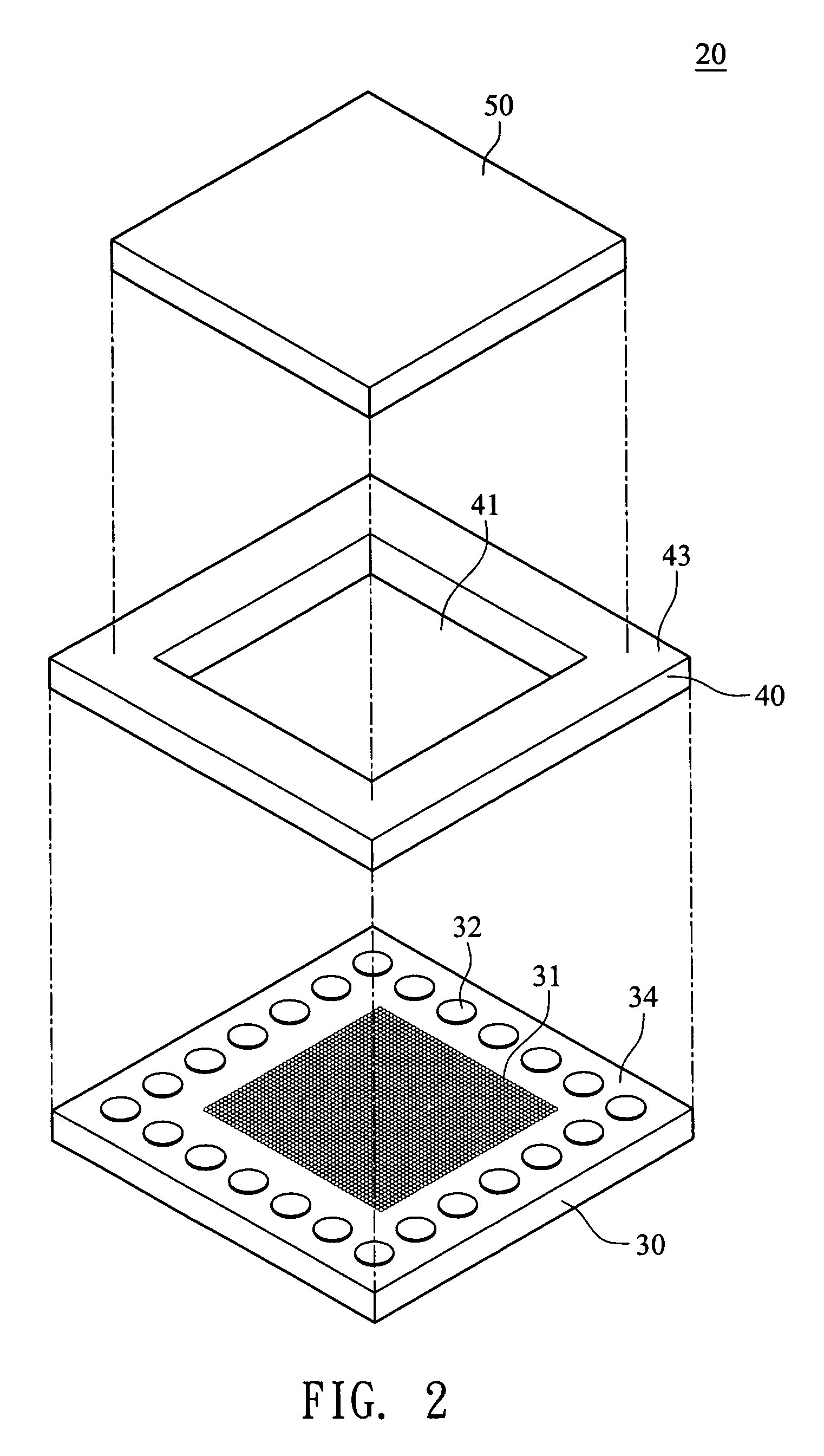
[0029]As can be seen in FIG. 2, the image sensor module package structure 20 with a supporting element of the first embodiment comprises a chip 30, the supporting element 40 and a light-transmitting element 50.

[0030]The chip 30 may be a complementary metal oxide semiconductor (CMOS) image sensor chip. As shown in FIG. 3, the chip 30 has a plurality of light-sensing elements 31, a plurality of first conducting pads 32, and at least one conducting channel 33.

[0031]The light-sensing elements 31 are arranged on a light-sensing area of a first surface 34, namely a top surface, of the chip 30 and serve to sense lights entering the image sensor module package structure 20. The first conducting pads 32 are arranged around the light-sensing area of the chip 30 and electrically connected to the light-sensing elements 31. The conducting channel 33 passes through the chip 30 so that one end thereof reveals at a second surface 35 of the chip 30, namely a bottom surface of the chip 30, while an o...


PUM


Abstract

An image sensor module package structure with a supporting element comprises a chip, the supporting element and a light-transmitting element. The chip has light-sensing elements arranged on a light-sensing area of a first surface thereof, first conducting pads electrically connected to the light-sensing elements, and a conducting channel passing through the chip and electrically connected to the first conducting pads at one end. The supporting element has an opening, a first coupling surface, and a second coupling surface. The opening corresponds to the light-sensing area and the first coupling surface is combined with the first surface of the chip while the light-transmitting element is combined with the second coupling surface. The supporting element separates the light-transmitting element from the chip by a proper distance, so as to enhance an image sensing accuracy of an image sensor module. The chip having the conducting channel effectively facilitates reducing an overall volume of the image sensor module package structure.

Description

BACKGROUND OF THE INVENTION[0001]1. Technical Field[0002]The present invention relates to an image sensor module package structure with a supporting element, and more particularly to an image sensor module package structure whose production yield is improved.[0003]2. Description of Related Art[0004]With the invention and popularization of various digital image products, a market demand for image sensor modules for being applied to these digital image products, such as digital cameras, camera phones, video phones, fingerprint readers, and so on, have been gradually increased. Generally speaking, image sensor modules, while using different light-sensing elements, can be classified into complementary metal oxide semiconductor (CMOS) image sensor modules and charge couple image sensor modules.[0005]Since the CMOS image sensor modules and the charge couple image sensor modules possess both advantages and disadvantages, respectively, they may be adopted in diverse applications according t...

Claims


Application Information

Patent Timeline
Patent Type & Authority Patents(United States)
IPC IPC(8): H01L31/0232
CPCH01L27/14685H01L27/14618H01L2224/13H01L2224/05024H01L2224/05022H01L2224/05548H01L2224/05001H01L2924/00014H01L24/02H01L2224/02377H01L2224/13024H01L2224/02372H01L2224/05599H01L2224/05099H01L27/146
Inventor HSIN, CHUNG-HSIENCHUANG, CHUN-HUAPENG, CHEN-PINCHANG, CHIEN-WEILIN, CHIEN-HEN
Owner KT IMAGING USA LLC
Why Eureka
Try Eureka