Array substrate and preparation method thereof

A technology for array substrates and capacitor areas, which is applied in semiconductor/solid-state device manufacturing, semiconductor devices, electrical components, etc., can solve problems that cannot meet design requirements, and achieve the goals of avoiding high deviation, reducing wiring space, and increasing capacitance Effect

Inactive Publication Date: 2015-04-29
KUNSHAN GO VISIONOX OPTO ELECTRONICS CO LTD
View PDF5 Cites 14 Cited by
  • Summary
  • Abstract
  • Description
  • Claims
  • Application Information

AI Technical Summary

Problems solved by technology

[0005] use figure 2 Although the method shown can increase the capacitance value, it still cannot meet the design requirements as the pixel size decreases

Method used


Image

  • Array substrate and preparation method thereof
  • Array substrate and preparation method thereof
  • Array substrate and preparation method thereof

Examples


Embodiment 1

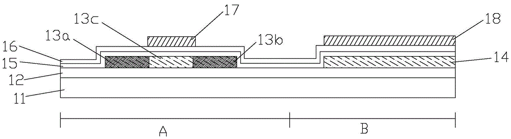
[0067] Figure 3A , 3B , 3C are cross-sectional views of pixels corresponding to the preparation method of etching away the first gate insulating layer by one-time exposure.

[0068] 1) if Figure 3A As shown, a buffer layer 12 covering the thin film transistor region A and the capacitor region B of the substrate is formed on the substrate 11, and the buffer layer 12 can be made of silicon dioxide (SiO 2 ) layer, and can also be formed by a double-layer buffer layer of silicon dioxide and silicon nitride (SiNx).

[0069] 2) An amorphous silicon layer is deposited on the buffer layer 12, and the amorphous silicon layer is crystallized to form a polysilicon layer, and photolithography is used to form the polysilicon layer corresponding to the thin film transistor above the thin film transistor region and the polysilicon layer corresponding to the capacitor above the capacitor region , and then P - Ion doping forms the thin film transistor semiconductor layer 13' and the capa...

Embodiment 2

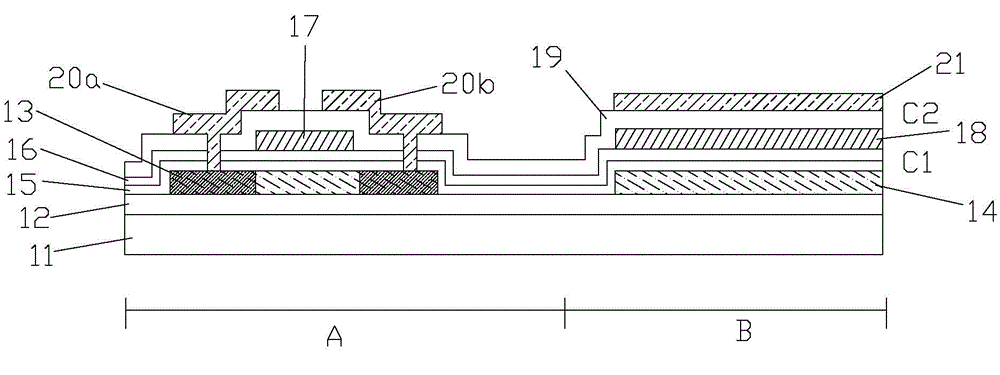
[0077] Figure 4A , Figure 4B Shown is a cross-sectional view of a pixel corresponding to the preparation method of etching away the first gate insulating layer by adopting a double exposure method. The preparation method is basically the same as that in Example 1, the difference is: step 3) coating photoresist on the semiconductor pattern layer, and then using a capacitively doped photomask to expose and develop, so that the photoresist in the thin film transistor region remains. Form the photoresist layer 41, the photoresist layer 41 covers the area except the capacitor semiconductor layer 14', and the capacitor semiconductor layer 14' is photoresisted. + Ion doping forms the first electrode 14; after peeling off the photoresist layer 41, an insulating layer 15' is formed on the semiconductor pattern layer, corresponding to the thin film transistor region and capacitor region covering the substrate, and then the insulating layer 15' is coated with photoresist , using the ...


PUM


Abstract

The invention discloses an array substrate and a preparation method thereof. The array substrate comprises a substrate, a buffer layer, a semiconductor pattern layer, a first grid electrode insulation layer, a second grid electrode insulation layer, a first conductive pattern layer, an interlayer insulation layer and a second conductive pattern layer, wherein the substrate comprises a thin-film transistor region and a capacitor region; the buffer layer is formed on the substrate; the semiconductor pattern layer is formed on the buffer layer and comprises a source and drain electrode region and a first electrode; the first grid electrode insulation layer is formed on the semiconductor pattern layer and correspondingly covers regions, except the first electrode, of the thin-film transistor region and the capacitor region; the second grid electrode insulation layer is formed on the first grid electrode insulation layer; the first conductive pattern layer is formed on the second grid electrode insulation layer and comprises a grid electrode and a second electrode; the interlayer insulation layer is formed on the first conductive pattern layer; the second conductive pattern layer is formed on the interlayer insulation layer and comprises a source electrode and a drain electrode which are coupled with the source and drain electrode region as well as a third electrode. With the adoption of the array substrate and the preparation method thereof, the capacitance of a capacitor is increased, film layer structures of the regions except the capacitor region are not changed, the signal line load is effectively decreased, and meanwhile, short-circuit risks of upper and lower film layers of the grid electrode insulation layers are reduced.

Description

technical field [0001] The invention relates to a low-temperature polysilicon (LTPS) array substrate and a preparation method thereof, in particular to an array substrate capable of effectively increasing capacitance and a preparation method thereof. Background technique [0002] In recent years, people have higher and higher requirements for the resolution of the display, and correspondingly, the space for wiring in the pixel is getting smaller and smaller. The capacitance in the pixel directly affects the electrical characteristics of the pixel and then affects the display characteristics. Therefore, the improvement in the limited layout space The capacitance value in the pixel is particularly important. [0003] Such as figure 1 , figure 2 As shown, it is a cross-sectional view of the film layer structure of capacitors and thin film transistors formed on an array substrate in a conventional way. figure 1 It includes a glass substrate 11, which is divided into a thin f...

Claims


Application Information

Patent Timeline
Patent Type & Authority Applications(China)
IPC IPC(8): H01L27/12H01L21/84H01L21/02H01L21/265
Inventor 岳明彦
Owner KUNSHAN GO VISIONOX OPTO ELECTRONICS CO LTD
Why Eureka
Try Eureka