Method for making grid oxidizing layer

A gate oxide layer and manufacturing method technology, which is applied in semiconductor/solid-state device manufacturing, electrical components, semiconductor devices, etc., can solve the problems of decreased transconductance and driving current capability, device performance degradation, and reduced N-type semiconductor, etc. The effect of increasing the thickness of the gate oxide at the drain end, reducing the vertical electric field strength, and mitigating adverse effects

Active Publication Date: 2009-10-21
SHANGHAI HUAHONG GRACE SEMICON MFG CORP
View PDF4 Cites 0 Cited by
  • Summary
  • Abstract
  • Description
  • Claims
  • Application Information

AI Technical Summary

Problems solved by technology

The hot carriers injected into the gate oxide layer can generate trap charges in the oxide layer, and generate interface states at the silicon-silicon dioxide interface of the device, resulting in degradation of device performance, such as threshold voltage drift, transconductance and Decreased drive current capability and increased subthreshold current
[0004] The hot carrier injection effect will reduce the turn-on current of N-type semiconductors, such as NMOS devices, and increase the turn-off current of P-type semiconductors, such as PMOS devices.

Method used


Image

  • Method for making grid oxidizing layer
  • Method for making grid oxidizing layer
  • Method for making grid oxidizing layer

Examples


Embodiment Construction

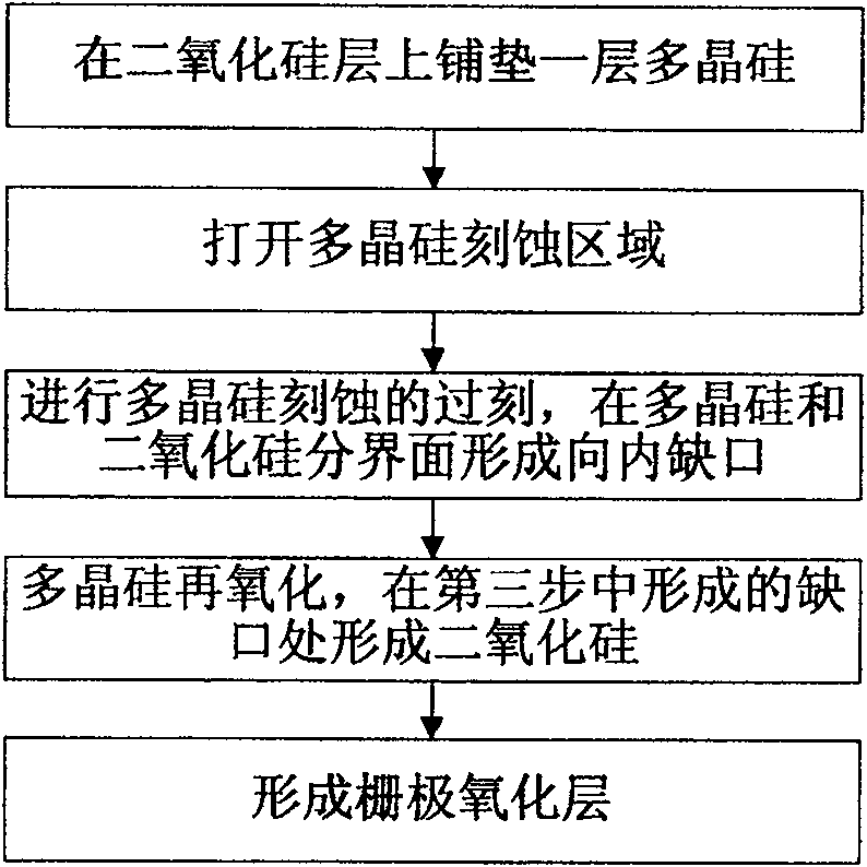
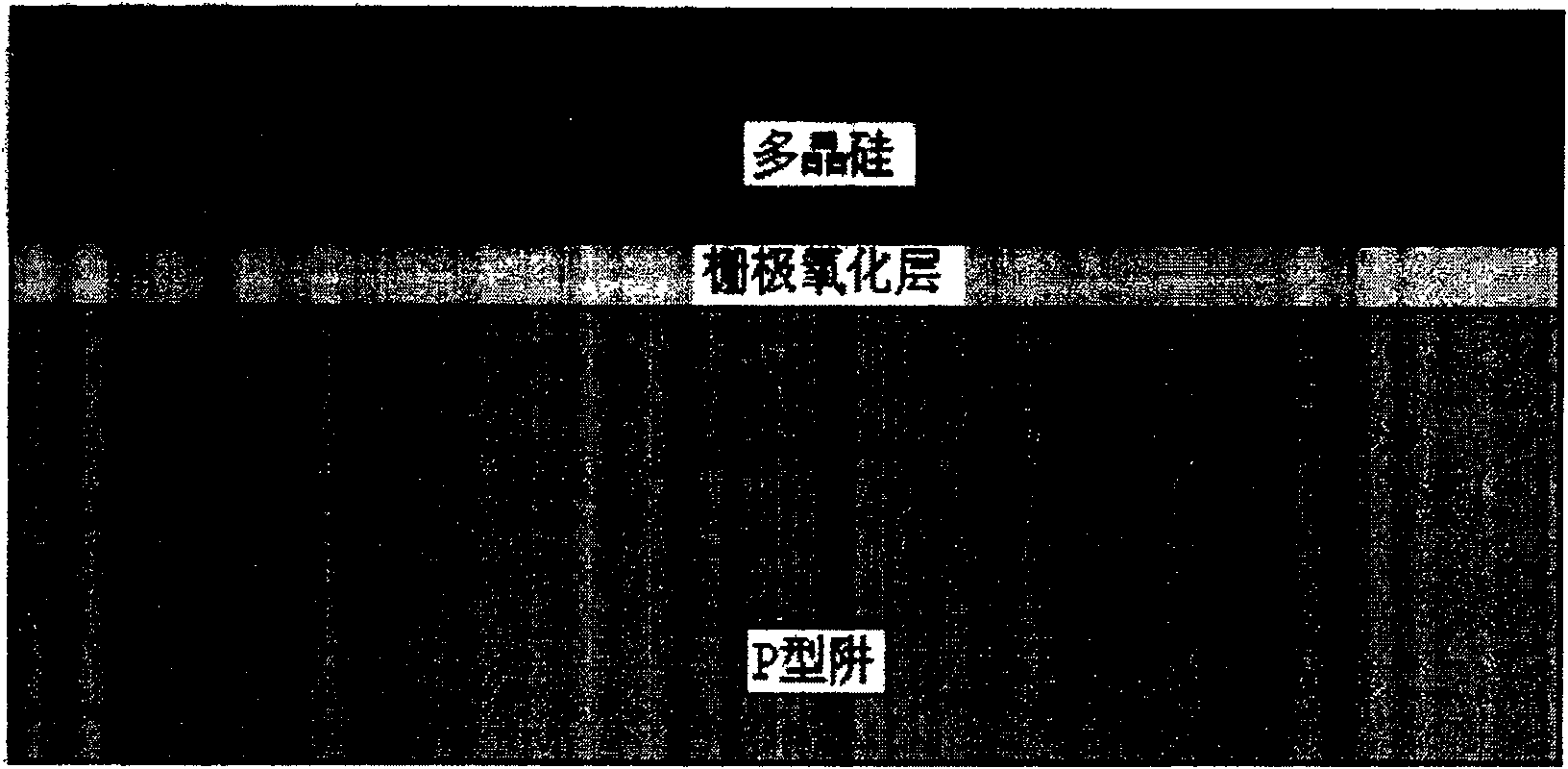
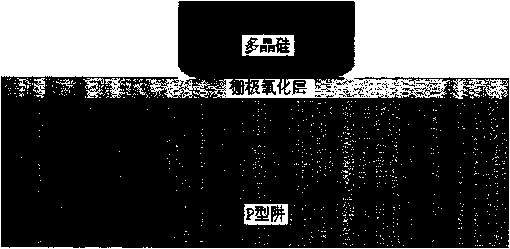
[0011] Such as figure 1 As shown, the gate oxide layer manufacturing method of the present invention includes the following steps: first, as figure 2 As shown, a layer of polysilicon is paved on the silicon dioxide layer on the P-type well, that is, the gate oxide layer, and the thickness of the paved silicon dioxide is between 1000 angstroms and 3000 angstroms according to different process requirements. Then, the polysilicon etching area is opened, and here the polysilicon etching area is opened by photolithography. Such as image 3 As shown, an inward gap is formed at the interface between polysilicon and silicon dioxide during polysilicon etching by dry etching. According to different process conditions, the depth of the inward notch in the horizontal direction does not exceed the boundary between the drain and the channel substrate. Next, if Figure 4 As shown, the polysilicon is re-oxidized, and silicon dioxide with a thickness of 30 angstroms to 150 angstroms is fo...


PUM


Abstract

The invention discloses a manufacturing method of a grid oxide layer, comprising the following steps: firstly, a polysilicon layer is laid on a silicon dioxide layer; secondly, a polysilicon etching zone is opened; thirdly, a polysilicon over etching is carried out to form an inward gap on the interface between the polysilicon layer and the silicon dioxide layer; fourthly, the polysilicon is oxidated again to form silicon dioxide on the gap formed in the third step; fifthly, a grid oxide layer is formed. By raising the leakage-end grid oxide thickness of component, the invention can control the injection effect of a hot carrier and slow down a bad impact on component capability by the hot-carried injection effect, so as to enhance the component capability.

Description

technical field [0001] The invention relates to the field of semiconductor manufacturing technology, in particular to a gate oxide layer manufacturing method in the field of semiconductor manufacturing technology. Background technique [0002] The hot carrier injection effect is a very well-known semiconductor effect. Hot carriers are conduction band electrons or valence band holes with high energy under the action of a strong electric field near the drain end of the MOS transistor. Hot carriers can be injected into the gate oxide layer of MOS transistors through various mechanisms, which is called hot carrier injection effect. The hot carrier injection effect will lead to silicon-silicon dioxide interface defects and hot carrier defects in silicon dioxide. The hot carrier injection effect has a prominent impact on the performance of semiconductor devices. [0003] Taking an NMOS device as an example, channel hot electron injection causes channel hot electrons to collide ...

Claims


Application Information

Patent Timeline
Patent Type & Authority Patents(China)
IPC IPC(8): H01L21/28H01L21/336
Inventor 陈晓波
Owner SHANGHAI HUAHONG GRACE SEMICON MFG CORP
Why Eureka
Try Eureka