Flip chip packaging structure with girth member and packaging method thereof

A flip-chip packaging and reinforcement technology, which is applied in the field of flip-chip packaging and its packaging, can solve problems such as inability to bond primer materials with solder bumps, chip substrates, poor packaging, and inability to solve packaging problems. Flux cleaning effect, reduction of poor coplanarity, and good encapsulation effect

Active Publication Date: 2009-10-21
ADVANCED SEMICON ENG INC
View PDF4 Cites 0 Cited by
  • Summary
  • Abstract
  • Description
  • Claims
  • Application Information

AI Technical Summary

Problems solved by technology

[0007] However, in the above-mentioned flip-chip packaging structure with stiffeners and its packaging technology in the prior art, the chip and the substrate must be electrically connected through solder bumps, and then the stiffeners are arranged on the substrate, and then filled with primer material. , although this can enhance the cleaning effect of the flux, but it cannot overcome the warpage of the substrate caused by reflow after the chip is mounted on the board
Because the design and configuration of stiffeners in the prior art still lead to packaging problems that cannot be solved, it cannot reduce the poor coplanarity of the flip-chip package, and at the same time, it cannot obtain good assistance in the flip-chip packaging process. Flux cleaning effect, but in the glue pouring process, it cannot effectively combine the primer material with the solder bump, chip and substrate to achieve the effect of protecting the chip
It can be seen that the existing semiconductor packaging technology still has room for further improvement.

Method used


Image

  • Flip chip packaging structure with girth member and packaging method thereof
  • Flip chip packaging structure with girth member and packaging method thereof
  • Flip chip packaging structure with girth member and packaging method thereof

Examples


Embodiment Construction

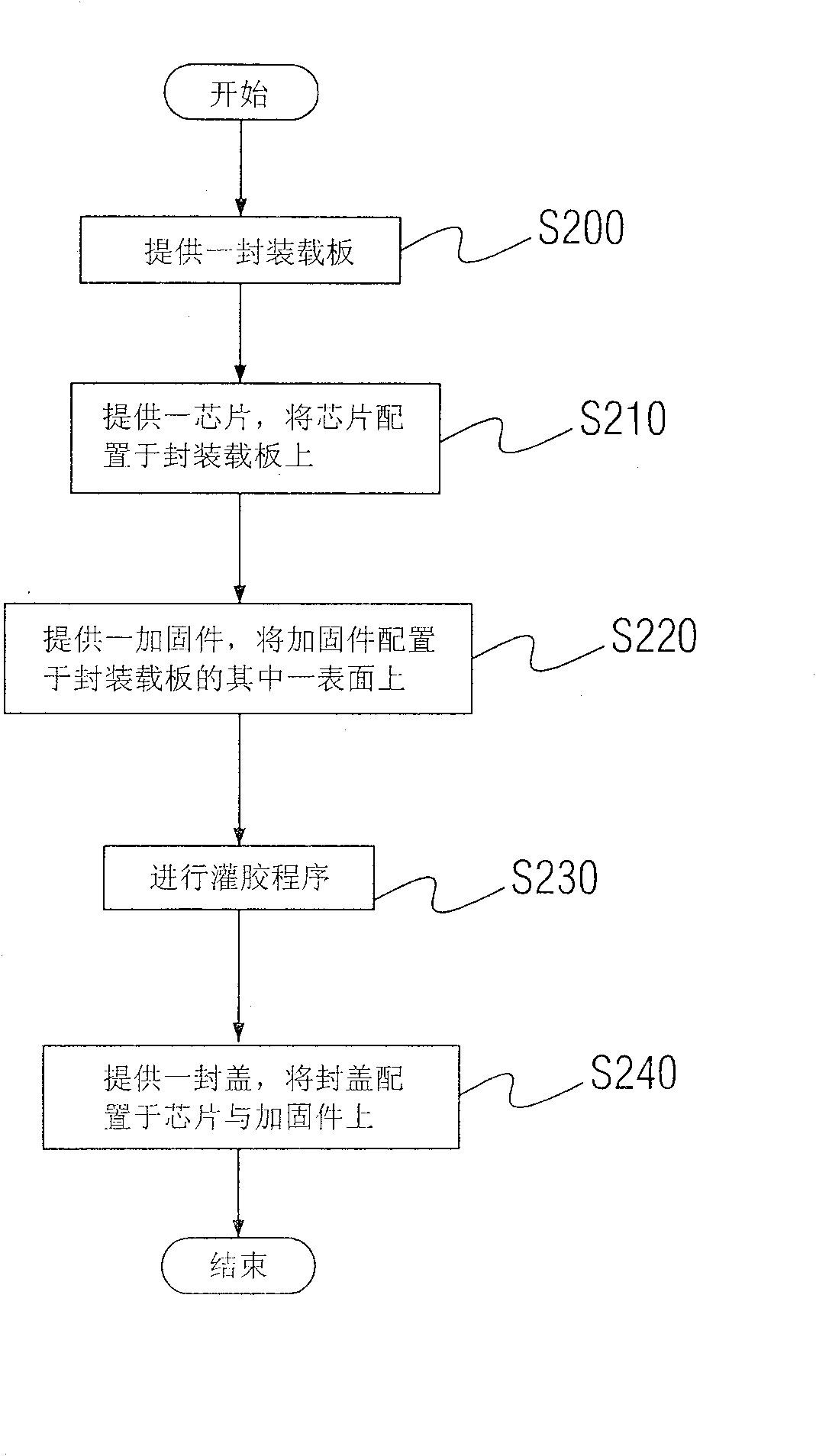
[0018] Hereinafter, preferred embodiments are specifically cited and described in detail in conjunction with the accompanying drawings:

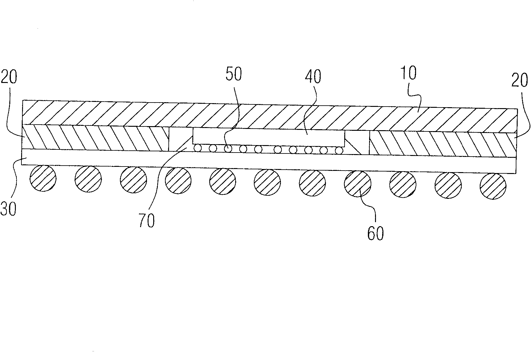
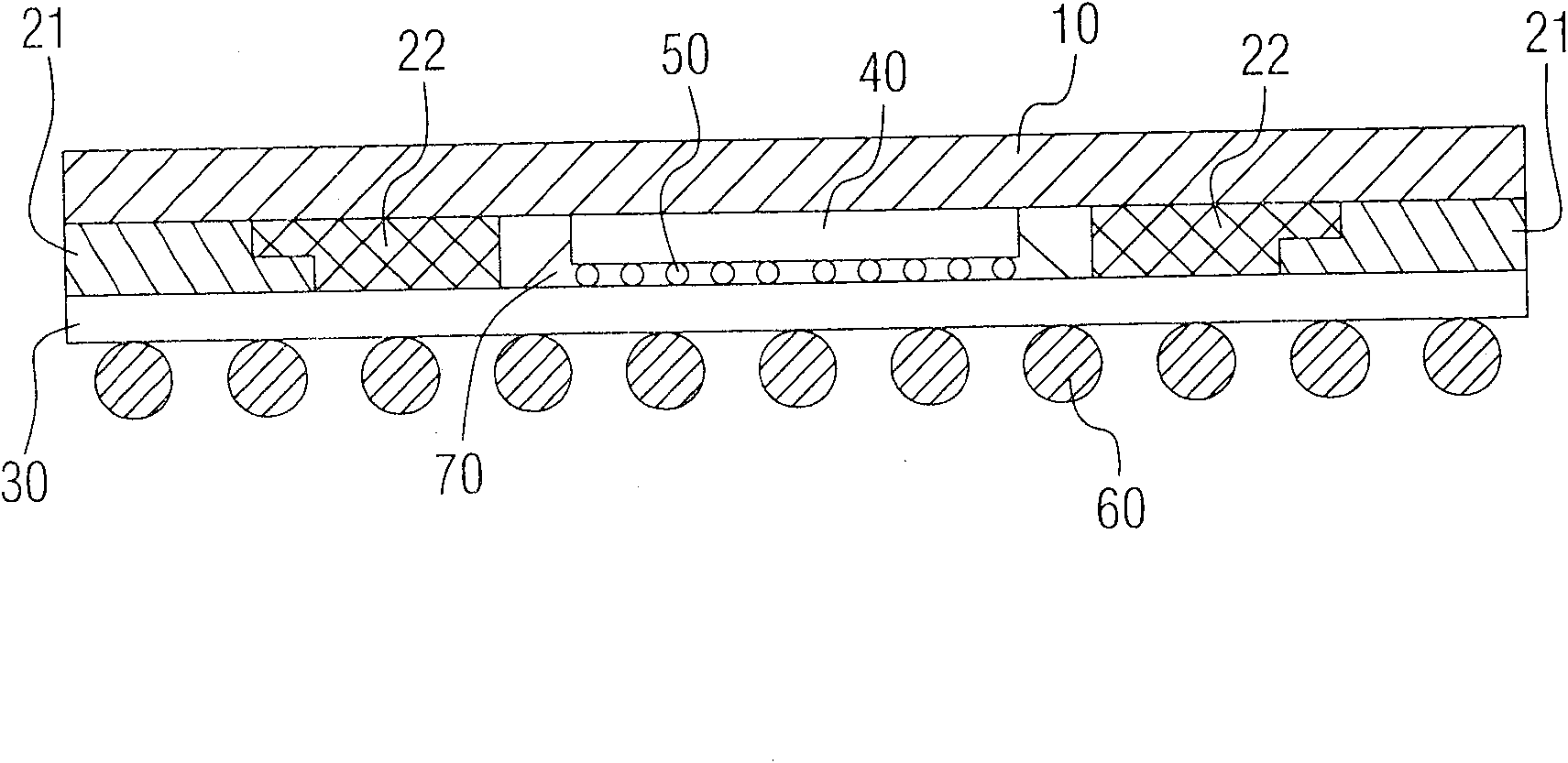
[0019] Please refer to image 3 as shown, image 3 It is a structural diagram of the flip-chip package of the present invention. The flip-chip package structure of the present invention includes: a package carrier 30, a first reinforcement, and several welding bumps 50, wherein the package carrier 30 is a circuit substrate; the first reinforcement The part 21 is arranged on one of the surfaces of the package carrier 30, the first reinforcement has an upper surface and a lower surface, and the first reinforcement is arranged on the upper surface of the package carrier with its lower surface, because the first The lower surface of the reinforcing element is larger than its upper surface, so that the first reinforcing element 21 is designed in two stages; and several welding bumps 50 are used to electrically connect the chip 40 and the package...


PUM


Abstract

The invention discloses a flip chip package structure with a strengthening part and a method for packing the same, wherein the flip chip package structure comprises a package carrier plate, a first strengthening part, a chip and a second strengthening part; the first strengthening part is arranged on the surface of the package carrier plate; the chip has a plurality of welding convex blocks to realize electrical connection between the chip and the package carrier plate; the second strengthening part which is also arranged on the surface of the package carrier plate is connected with the first strengthening part; moreover, the first strengthening part is arranged outside the second strengthening part.

Description

technical field [0001] The invention relates to a flip-chip packaging structure and a packaging method thereof, in particular to a flip-chip packaging structure with reinforcements and packaging technology. Background technique [0002] In recent years, under the strong demand for electronic products to be light, thin, and small, chip packaging has been developing towards high-speed processing and miniaturization of electronic products. Therefore, high-speed processing and miniaturization are undoubtedly the goals pursued by chip packages. [0003] Based on the above reasons, the flip-chip package came into being. The difference between it and the traditional wire bonding package is that the flip-chip package is to place the surface of the chip with the electronic circuit on the substrate in an upside-down manner, and at the same time electrically connect it with solder bumps. To the substrate, this can effectively reduce the size of the package, and handle high-speed signal...

Claims


Application Information

Patent Timeline
Patent Type & Authority Patents(China)
IPC IPC(8): H01L23/16H01L21/50
CPCH01L2224/73253H01L2924/15311H01L2224/73204H01L2224/16225H01L2224/32225H01L23/16H01L2924/00012H01L2924/00
Inventor 陈昭雄
Owner ADVANCED SEMICON ENG INC
Why Eureka
Try Eureka