A semiconductor component packaging equipment applicable to different types and specifications

A kind of packaging equipment and semiconductor technology, applied in the direction of packaging, transportation and packaging, single objects, etc., can solve the problems of unable to meet the packaging work of multiple types and specifications of semiconductor components, and reduce output efficiency

Active Publication Date: 2020-09-18
江苏尖端半导体有限公司
View PDF7 Cites 0 Cited by
  • Summary
  • Abstract
  • Description
  • Claims
  • Application Information

AI Technical Summary

Problems solved by technology

[0003] Semiconductor components need to be transported for short or long distances after production, so semiconductor components need to be packaged during transportation, and the packaging tube with a long strip structure is used to prevent them from being damaged during transportation. Collision damage and static damage to semiconductor components; general manufacturers produce semiconductor components of different types and specifications in the production of semiconductor components, and traditional automatic packaging equipment for semiconductor components cannot meet the requirements of various types and specifications of semiconductor components Packaging work, which leads to a decrease in the overall output efficiency of the manufacturer

Method used


Image

  • A semiconductor component packaging equipment applicable to different types and specifications
  • A semiconductor component packaging equipment applicable to different types and specifications
  • A semiconductor component packaging equipment applicable to different types and specifications

Examples


Embodiment Construction

[0038] Below in conjunction with accompanying drawing and embodiment of description, specific embodiment of the present invention is described in further detail:

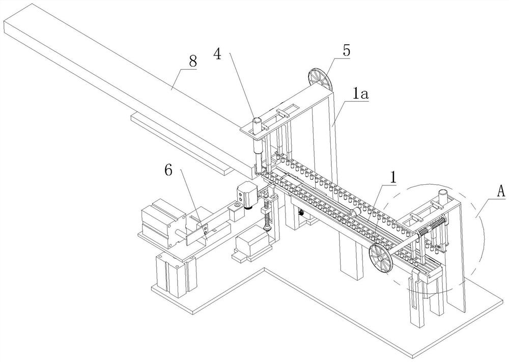
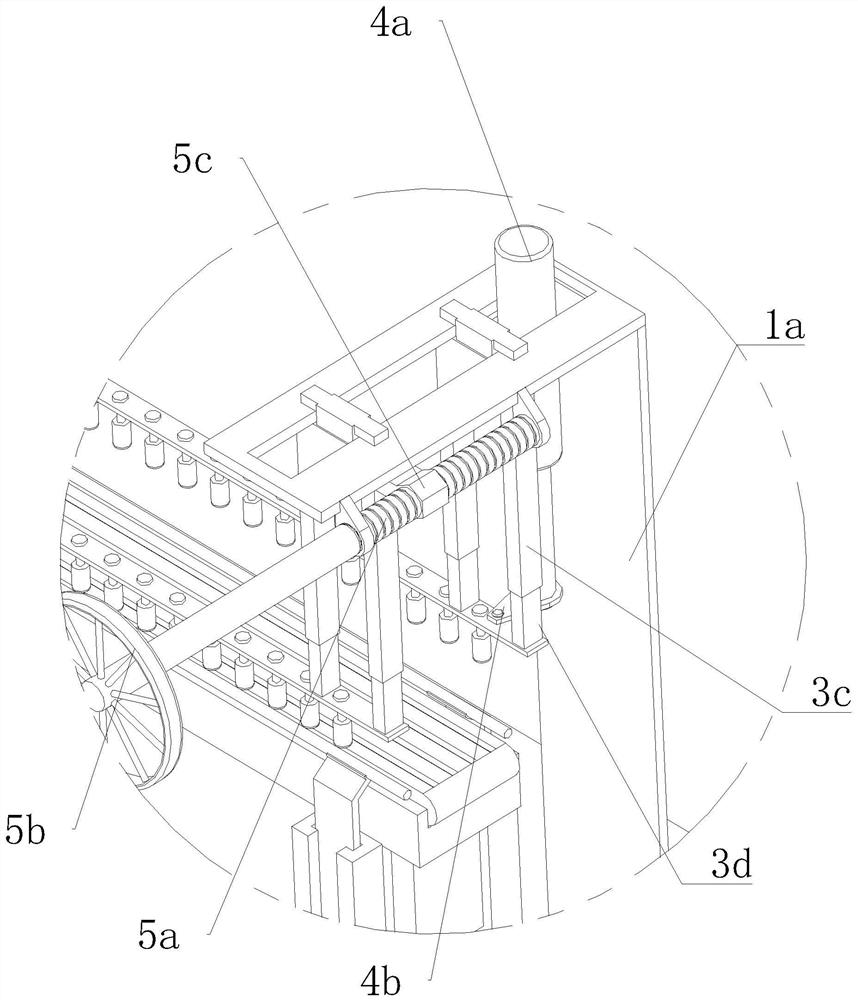
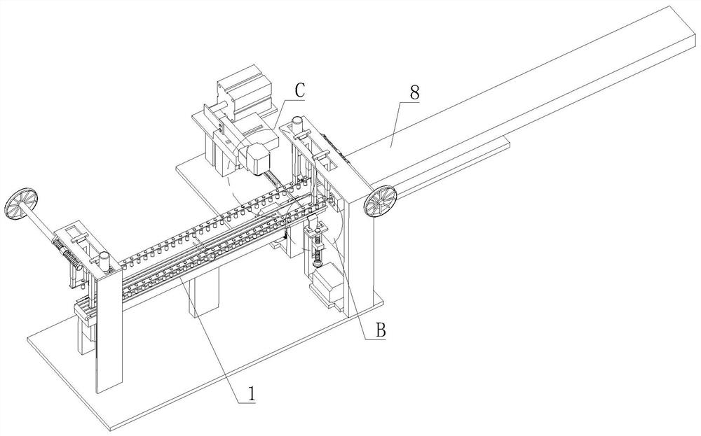
[0039] refer to Figure 1 to Figure 14 The one shown can be applied to semiconductor component packaging equipment of different types and specifications, including a stepping conveyor belt 1, a guiding device, a limiting device and a feeding device 6, and the guiding device includes two respectively arranged on the stepping conveyor belt 1- The light guide rods 2 on the side, each guide light rod 2 can be vertically movable through a lifting device, and the limit device includes two guide assemblies respectively arranged on one side of the stepping conveyor belt 1, each guide assembly is always located at the stepping Above the type conveyor belt 1, each guide assembly can be vertically movable through a height fine-tuning device 4, and the two guide assemblies can also be moved toward or away from each other throug...


PUM


Abstract

The invention relates to the field of packaging of semiconductor elements, in particular to packaging equipment applicable to semiconductor elements of different types and specifications. The equipment comprises a stepping conveying belt, a guiding device, a limiting device and a feeding device; the guiding device comprises two guiding polish rods which are arranged at one sides of the stepping conveying belt respectively, each guiding polish rod can move vertically through one lifting device, and the limiting device comprises two guide assemblies which are arranged at one sides of the stepping conveying belt respectively; each guide assembly is always located above the stepping conveying belt and can vertically move through a height fine-adjustment device, the two guide assemblies can bemovably arranged face to face or back to back through spacing fine-adjustment devices, and the feeding device is arranged outside one side of the downstream end of the stepping conveying belt. The equipment can be applicable to automatically packaging the semiconductor elements of different types and specifications, and the product output efficiency of manufacturers is greatly improved.

Description

technical field [0001] The invention relates to the field of semiconductor element packaging, in particular to semiconductor element packaging equipment applicable to different types and specifications. Background technique [0002] A semiconductor component is an electronic component whose conductivity is between a good conductor and an insulator. It uses the special electrical characteristics of semiconductor materials to complete specific functions. It can be used to generate, control, receive, transform, amplify signals and perform energy conversion. The semiconductor of semiconductor components The material is silicon, germanium or gallium arsenide, which can be used as rectifiers, oscillators, light emitters, amplifiers, photometers and other equipment. [0003] Semiconductor components need to be transported for short or long distances after production, so semiconductor components need to be packaged during transportation, and the packaging tube with a long strip stru...

Claims


Application Information

Patent Timeline
Patent Type & Authority Patents(China)
IPC IPC(8): B65B5/10B65B35/44B65B59/00
CPCB65B5/10B65B35/44B65B59/00
Inventor 王茜史彦文卞杰锋
Owner 江苏尖端半导体有限公司
Why Eureka
Try Eureka