Fabrication of lean-free stacked capacitors

a technology of stacked capacitors and stacked plates, which is applied in the direction of conveying, food shaping, transportation and packaging, etc., can solve the problems of 146/b>, the width and thickness of the support beams are more difficult to control in the prior art, and the malfunction of the dram is more difficult to achiev

Inactive Publication Date: 2006-09-21
KIM E E +3
View PDF3 Cites 48 Cited by
  • Summary
  • Abstract
  • Description
  • Claims
  • Application Information

AI Technical Summary

Benefits of technology

[0025] In this manner, the support structures for preventing leaning of the first electrodes of the stacked capacitors are formed after the first electrodes are fabricated within the openings. Thus, less subsequent etching steps do not deteriorate the structural integrity of the support structures. In addition, because the first electrodes are available for forming the support structures, masking spacers are formed using the first electrodes for easily patterning the support structures around the first electrodes.

Problems solved by technology

Such exposed and leaning electrodes 116 and 122 when disposed close enough together may disadvantageously contact each-other during fabrication resulting in malfunction of the DRAM.
Thus, the width and the thickness of the support beams 146 are more difficult to control in the prior art.

Method used


Image

  • Fabrication of lean-free stacked capacitors
  • Fabrication of lean-free stacked capacitors
  • Fabrication of lean-free stacked capacitors

Examples


Embodiment Construction

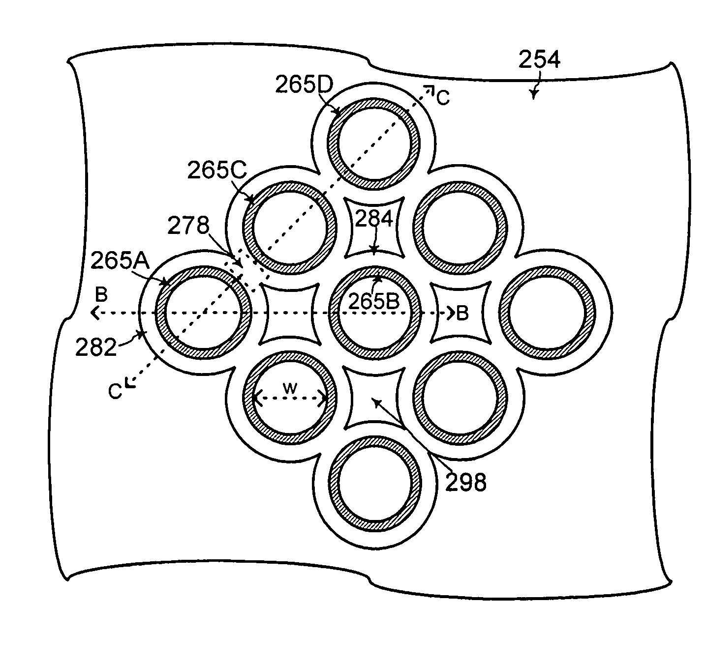
[0043] Referring to FIG. 8, a DRAM (dynamic random access memory) is fabricated onto a semiconductor substrate 202, comprised of a silicon wafer for example. FIGS. 9A, 10A, 11A, 12A, 13A, 14A, 15A, 16A, 18A, 19A, 20A, 21A, and 23A show cross-sectional views along a B-B direction of FIG. 8 for fabrication of stacked capacitors, according to an embodiment of the present invention. FIGS. 9B, 10B, 11B, 12B, 13B, 14B, 15B, 16B, 18B, 19B, 20B, 21B, and 23B show cross-sectional views along a C-C direction of FIG. 8 for fabrication of stacked capacitors, according to an embodiment of the present invention.

[0044] In an example embodiment of the present invention, the stacked capacitors are part of the DRAM fabricated on the semiconductor substrate 202. The B-B direction of FIG. 8 crosses through a plurality of word-lines of such a DRAM, and the C-C direction of FIG. 8 crosses through a plurality of bit-lines of such a DRAM.

[0045] Referring to FIGS. 9A and 9B, a plurality of STI (shallow tr...


PUM


Abstract

For fabricating lean-free stacked capacitors, openings are formed through layers of materials including a layer of support material displaced from a bottom of the openings. A respective first electrode is formed for a respective capacitor within each of the openings. The layer of support material is patterned to form support structures around the first electrodes. Masking spacers are formed around exposed top portions of the first electrodes, and exposed portions of the support material are etched away to form the support structures. Such stacked capacitors are applied within a DRAM (dynamic random access memory).

Description

CROSS-REFERENCE TO RELATED APPLICATION(S) [0001] The present application is a divisional of an earlier filed copending patent application with Ser. No. 10 / 853,628 filed on May 25, 2004, for which priority is claimed. This earlier filed copending patent application with Ser. No. 10 / 853,628 is in its entirety incorporated herewith by reference. [0002] The present application claims priority under 35 U.S.C. § 119 to Korean Patent Application No. P2004-8770, filed on Feb. 10, 2004, which is incorporated herein by reference in its entirety. A certified copy of Korean Patent Application No. P2004-8770 is contained in the parent copending patent application with Ser. No. 10 / 853,628.TECHNICAL FIELD [0003] The present invention relates generally to integrated circuit fabrication, and more particularly, to fabrication of lean-free stacked capacitors that may be used for DRAM (dynamic random access memory). BACKGROUND OF THE INVENTION [0004]FIG. 1 shows a simplified schematic of a DRAM (dynami...

Claims


Application Information

Patent Timeline
Patent Type & Authority Applications(United States)
IPC IPC(8): H01L21/82H01L21/02H01L21/8242H01L27/02H01L27/108H01L29/92
CPCH01L27/0207H01L28/91H01L27/10855H01L27/10852H10B12/033H10B12/0335A23L7/10A23P30/00B65G21/12
Inventor KIMHUH, MINSHIN, DONG-WONLEE, BYEONG-HYEON
Owner KIM E E
Why Eureka
Try Eureka