Composite display drive method of shadow mask type plasma display board
A plasma and composite display technology, applied to static indicators, instruments, identification devices, etc., can solve the problems of low brightness, high maintenance voltage, and low efficiency of opposite discharge
- Summary
- Abstract
- Description
- Claims
- Application Information
AI Technical Summary
Problems solved by technology
Method used
Image

Examples
Embodiment 2
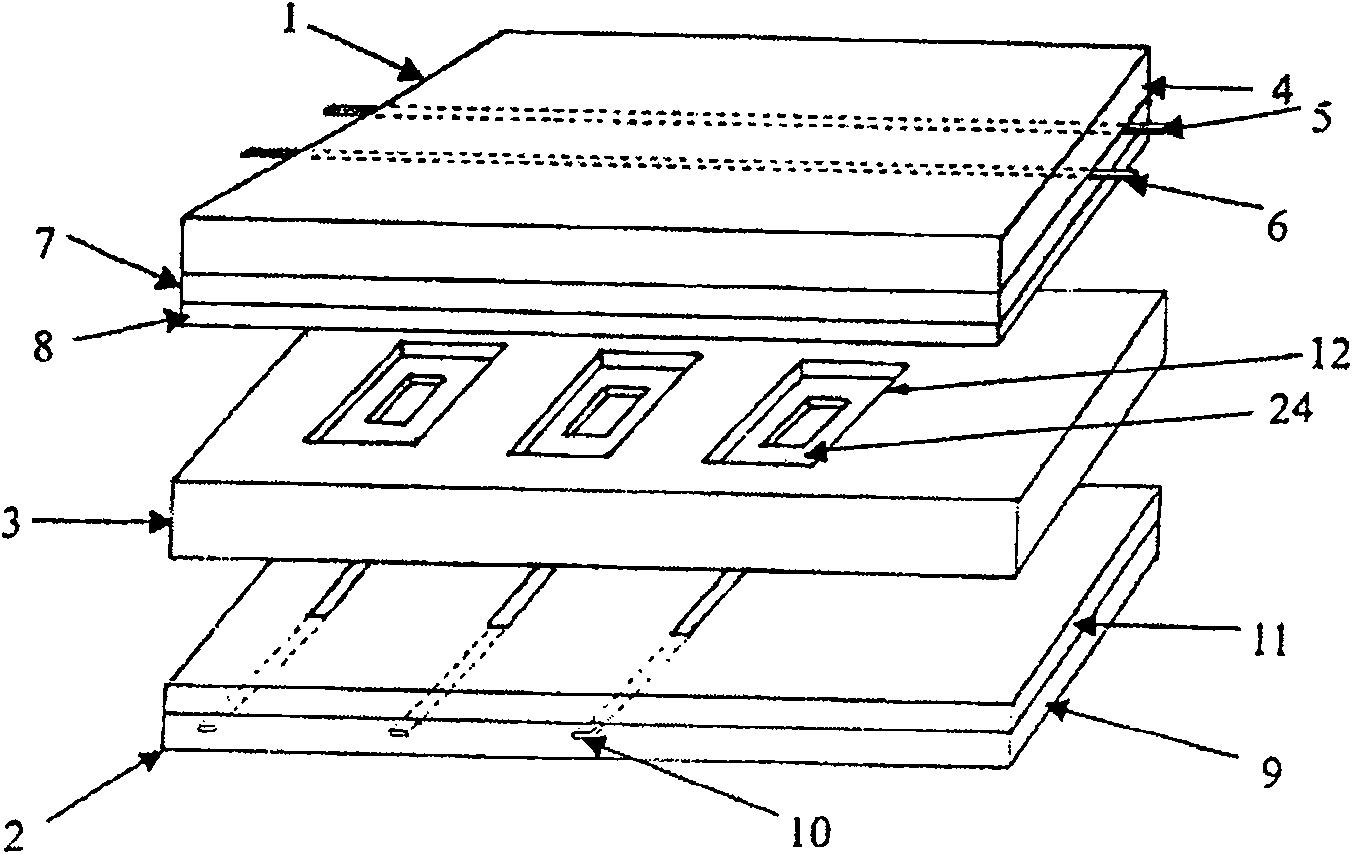
[0022] Such as figure 1 , 4 shown.
[0023] Such as figure 1The three-electrode shadow mask plasma display panel shown includes a front substrate 1, a rear substrate 2, and a shadow mask 3, wherein the shadow mask 3 is packaged between the front and rear substrates 1 and 2, and the front substrate 1 is mainly composed of the front substrate Glass substrate 4, first electrode pairs 5, 6, dielectric layer 7, protective film 8, wherein the first electrode pairs 5, 6 are arranged in parallel on the front substrate glass substrate 4, it can be formed without transparent conductive film ITO electrode, electrode 5 is called sustain electrode, electrode 6 is called scan electrode, dielectric layer 7 is covered on the first electrode pair 5, 6, and protective film 8 is covered on the dielectric layer 7; Substrate glass substrate 9, second electrode 10, dielectric layer 11, wherein the second electrode 10 is located on the rear substrate glass substrate 9, the dielectric layer 11 cov...
Embodiment 3
[0027] Such as figure 1 , 5 shown.
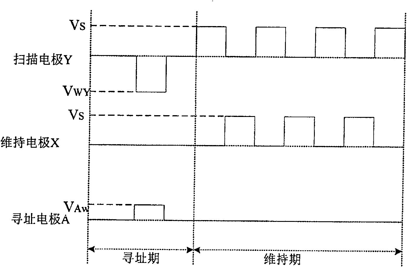
[0028] exist figure 1 In the shown three-electrode shadow mask plasma display panel, the scan electrodes and the sustain electrodes of the front substrate 1 and the address electrodes of the rear substrate 2 are applied as follows Figure 5 As shown in the drive waveform, the shadow mask is applied with a floating potential. During the addressing period, the scan electrodes apply a negative voltage pulse V wy , the addressing electrode applies a positive voltage pulse V a , the sustain electrode is connected to 0V voltage (V wy with V a The sum is greater than the ignition voltage between the scanning electrode and the addressing electrode), the addressing discharge makes the pixels selected in this row enter the ignited state, and after scanning all rows, the addressing of the subfield to the entire screen pixels is completed. Positive wall charges are accumulated on the dielectric layer of the scan electrodes, negative wall charges...
PUM
| Property | Measurement | Unit |
|---|---|---|
| thickness | aaaaa | aaaaa |
Abstract
Description
Claims
Application Information
 - R&D
- Intellectual Property
- Life Sciences
- Materials
- Tech Scout
- Unparalleled Data Quality
- Higher Quality Content
- 60% Fewer Hallucinations
Browse by: Latest US Patents, China's latest patents, Technical Efficacy Thesaurus, Application Domain, Technology Topic, Popular Technical Reports.
© 2025 PatSnap. All rights reserved.Legal|Privacy policy|Modern Slavery Act Transparency Statement|Sitemap|About US| Contact US: help@patsnap.com