Thin-film transistor substrate, electronic device and preparation method thereof

A technology of thin-film transistors and substrates, applied in transistors, semiconductor/solid-state device manufacturing, circuits, etc., can solve problems such as poor electrical uniformity, and achieve the effect of good electrical uniformity

Active Publication Date: 2009-12-30
AU OPTRONICS CORP
View PDF4 Cites 0 Cited by
  • Summary
  • Abstract
  • Description
  • Claims
  • Application Information

AI Technical Summary

Problems solved by technology

[0009] The invention provides a thin film transistor array substrate, which can improve the problem of poor electrical uniformity

Method used


Image

  • Thin-film transistor substrate, electronic device and preparation method thereof
  • Thin-film transistor substrate, electronic device and preparation method thereof
  • Thin-film transistor substrate, electronic device and preparation method thereof

Examples


Embodiment Construction

[0085] The technical solutions of the present invention will be further described in more detail in conjunction with the accompanying drawings and specific embodiments.

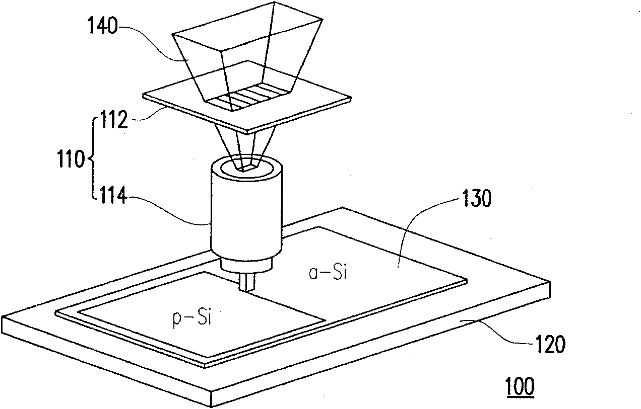
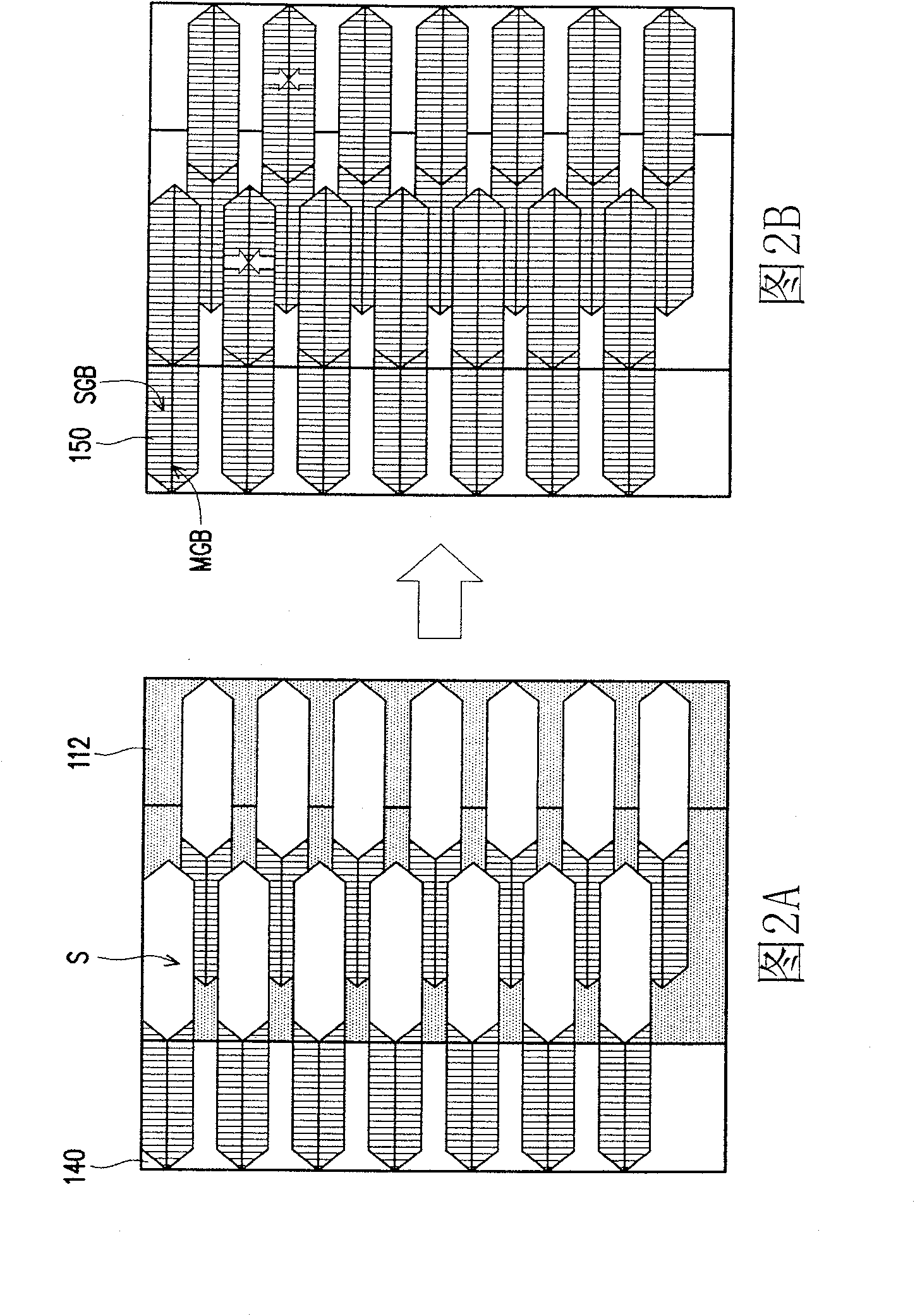
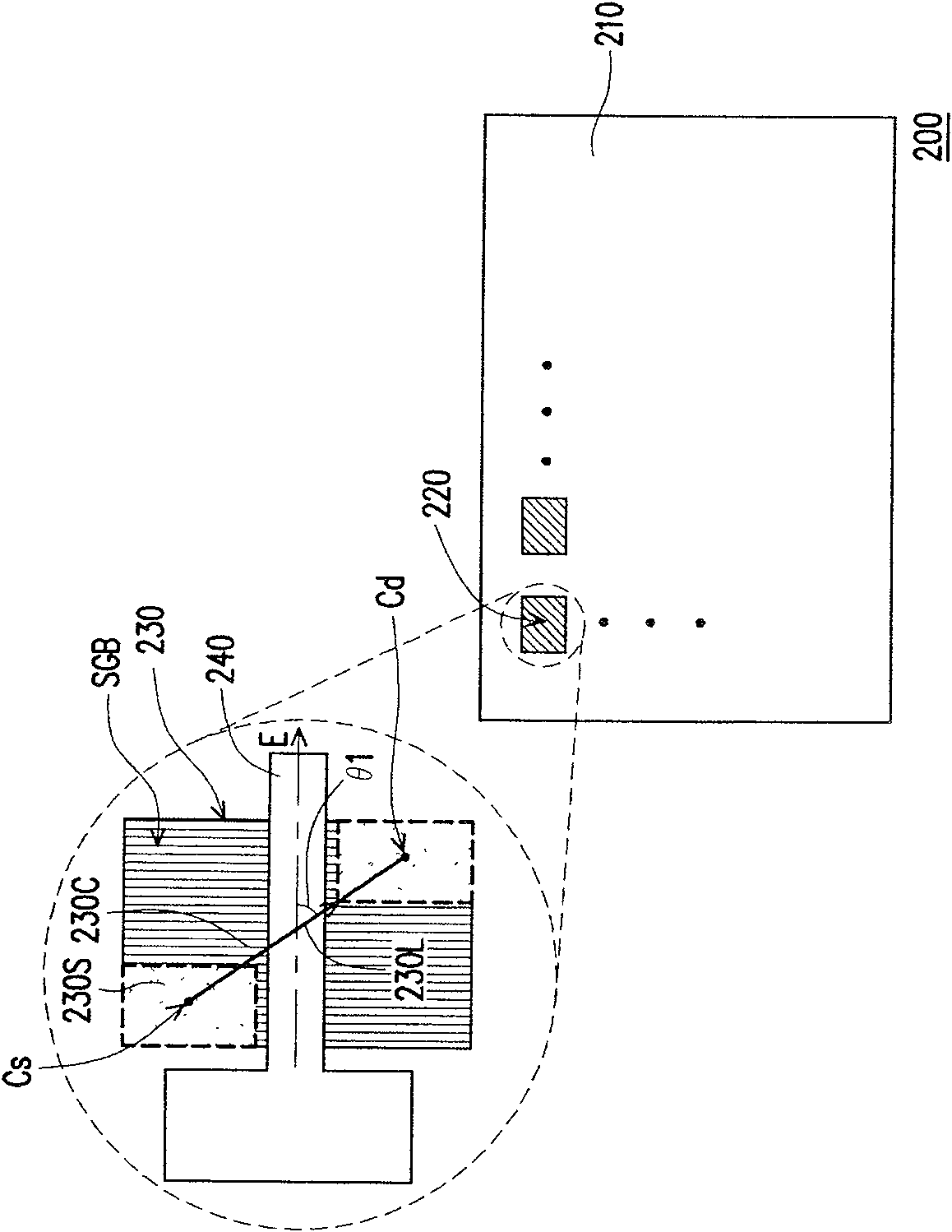
[0086] image 3 It is a schematic top view and a partially enlarged view of the thin film transistor array substrate according to the first embodiment of the present invention. Please refer to image 3 , the thin film transistor array substrate 200 includes a substrate 210 and at least one thin film transistor 220 disposed on the substrate 210, wherein the thin film transistor 220 includes a semiconductor island 230 and at least one gate 240, and the semiconductor island 230 has a source region 230S, The drain region 230D and the channel region 230C located between the source region 230S and the drain region 230D, wherein the material of the semiconductor island 230 can be polycrystalline, monocrystalline or microcrystalline composed of silicon; Or the polycrystalline form, single crystal form or microcryst...


PUM


Abstract

The invention discloses a thin-film transistor substrate, which comprises a backing material, and at least one thin-film transistor arranged on the backing material; wherein the thin-film transistor comprises a semiconductor island and at least one grid electrode. The semiconductor island has a source electrode region, a drain electrode region, a passage region positioned therebetween, and a plurality of secondary grain boundaries. In a region of the grid electrode corresponding to the passage region, a first included angle, which is substantially not a 90 DEG C, is formed between a line for connecting the source electrode region center with the drain electrode region center and an extension direction of the grid electrode, and a second included angle, which is substantially not a 0 or 90 DEG C, is formed between a line for connecting the source electrode region center with the drain electrode region center and the secondary grain boundaries of the passage region. In addition, the invention provides a manufacturing method of the thin-film transistor substrate, an electronic device and a manufacturing method thereof.

Description

technical field [0001] The present invention relates to a thin film transistor substrate, an electronic device and the above manufacturing method, in particular to a thin film transistor substrate with sub-grain boundary design in the channel region, the electronic device and the above manufacturing method. Background technique [0002] In recent years, with the increasing maturity of optoelectronic technology and semiconductor manufacturing technology, flat-panel displays have flourished. Among them, liquid crystal displays have gradually replaced traditional cathodes based on their advantages of low-voltage operation, no radiation scattering, light weight, and small size. Ray tube displays have become the mainstream of display products in recent years. [0003] In general, liquid crystal displays can be classified into two types: amorphous silicon thin film transistor liquid crystal displays and low temperature poly-silicon thin film transistor liquid crystal displays. Co...

Claims


Application Information

Patent Timeline
Patent Type & Authority Patents(China)
IPC IPC(8): H01L29/786H01L29/41H01L29/10H01L27/12H01L21/336H01L21/84
Inventor 孙铭伟赵志伟
Owner AU OPTRONICS CORP
Why Eureka
Try Eureka