Phase change memory and manufacturing method thereof

A manufacturing method and phase change technology, applied in static memory, digital memory information, information storage, etc., can solve the problems of heating efficiency, contact surface electrical uniformity limitation, etc.

Inactive Publication Date: 2008-09-03
IND TECH RES INST +4
View PDF1 Cites 4 Cited by
  • Summary
  • Abstract
  • Description
  • Claims
  • Application Information

AI Technical Summary

Problems solved by technology

However, in this structure, the part that forms the electrical connection path is a hole-filling process, which has considerable limitations in terms of heating efficiency and electrical uniformity of the contact surface.

Method used


Image

  • Phase change memory and manufacturing method thereof
  • Phase change memory and manufacturing method thereof
  • Phase change memory and manufacturing method thereof

Examples


Embodiment Construction

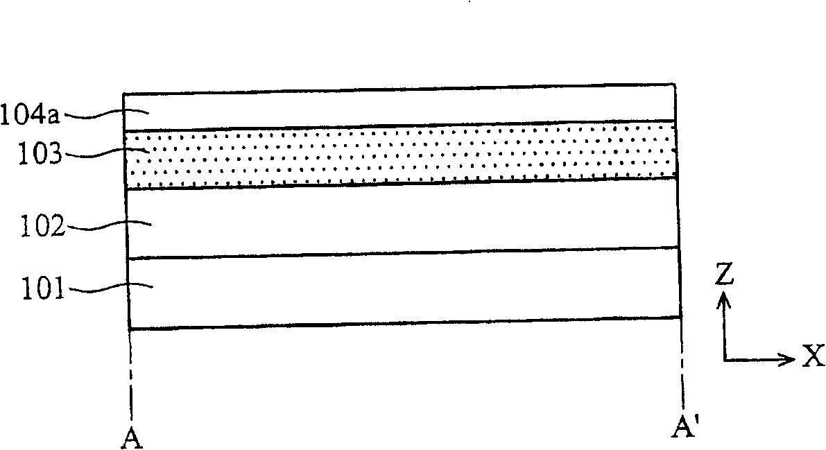
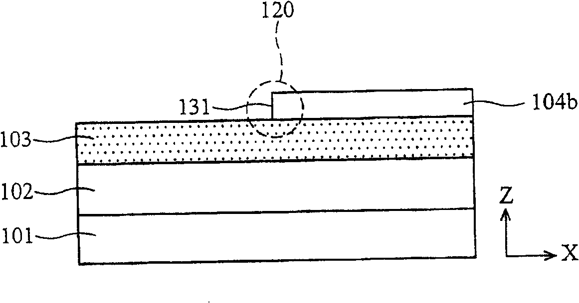
[0092] Hereinafter, a method for manufacturing a phase change memory according to an embodiment of the present invention will be described in detail with reference to the drawings. Figure 2a~2s is the cross-sectional flow chart of the phase change memory along the X axis, Figure 3a~3s is the cross-sectional flow chart of the phase change memory along the Y axis, and Figure 4a~4s For the phase change memory top view flow chart, in addition, Figure 2a~2s for along Figure 4a~4s The profile of the A-A' tangent line, and Figure 3a~3s for along Figure 4a~4s Sectional view of the B-B' tangent.

[0093] First, please refer to Figure 2a , 3a , and 4a, sequentially forming a first electrode layer 102, a phase change layer 103, and a dielectric layer 104a on a base 101, wherein the base 101 can be a substrate used in a semiconductor process, such as Silicon substrate. The substrate 101 can be a substrate that has completed the CMOS front-end process, and may also include ...


PUM


Abstract

The method relates to a phase change memory and a method for manufacturing the same. The phase change memory includes: a substrate; a first electrode layer formed on the substrate; a dot shape phase change post formed on the first electrode layer; a dielectric layer formed on the first electrode layer which covers the dot shape phase change post side, and exposes the dot shape phase change post upper surface; and a second electrode layer formed on the dielectric layer and the dot shape phase change post, therein, two-dimensional of the dot shape phase change post upper surface also is less than exposal limit.

Description

technical field [0001] The present invention relates to a phase-change memory and a manufacturing method thereof, in particular to a phase-change memory that reduces the contact area between a phase-change layer and an electrode and a manufacturing method thereof. Background technique [0002] Phase change memory has the characteristics of high read speed, low power, high capacity, high reliability, high write and erase times, low operating voltage / current and low cost, and is very suitable for combining with CMOS technology and can be used as a higher density Stand-alone or embedded memory applications are currently very promising next-generation new memories. Due to the unique advantages of phase change memory technology, it is also considered to be very likely to replace the current commercially competitive SRAM and DRAM volatile memory and Flash non-volatile memory technology, and it is expected to become a new generation with great potential in the future semiconductor...

Claims


Application Information

Patent Timeline
Patent Type & Authority Applications(China)
IPC IPC(8): H01L45/00H01L27/24G11C11/56
Inventor 卓言
Owner IND TECH RES INST
Why Eureka
Try Eureka