Silica tube for growing semi-insulated gallium arsenide and method for doping carbon in gallium arsenide

A gallium arsenide and quartz tube technology, which is applied in the VGF field of high-performance compound semiconductor SI-GaAs single crystal, can solve the problems of atmosphere doping and quartz tube structure that cannot be satisfied.

Inactive Publication Date: 2009-12-16
INST OF SEMICONDUCTORS - CHINESE ACAD OF SCI
View PDF0 Cites 20 Cited by
  • Summary
  • Abstract
  • Description
  • Claims
  • Application Information

AI Technical Summary

Problems solved by technology

However, under the vertical gradient solidification process of the quartz tube-PBN system currently used, it is difficult to achieve atmosphere doping
First, there is no contact with ℃ in the entire growth syst

Method used


Image

  • Silica tube for growing semi-insulated gallium arsenide and method for doping carbon in gallium arsenide
  • Silica tube for growing semi-insulated gallium arsenide and method for doping carbon in gallium arsenide
  • Silica tube for growing semi-insulated gallium arsenide and method for doping carbon in gallium arsenide

Examples


Embodiment Construction

[0028] The purpose of the present invention is to provide an atmosphere C-doped method for growing semi-insulating gallium arsenide by the vertical gradient solidification technology of the quartz tube-PBN system, which has the advantages of easier control of C concentration and better electrical uniformity of the material.

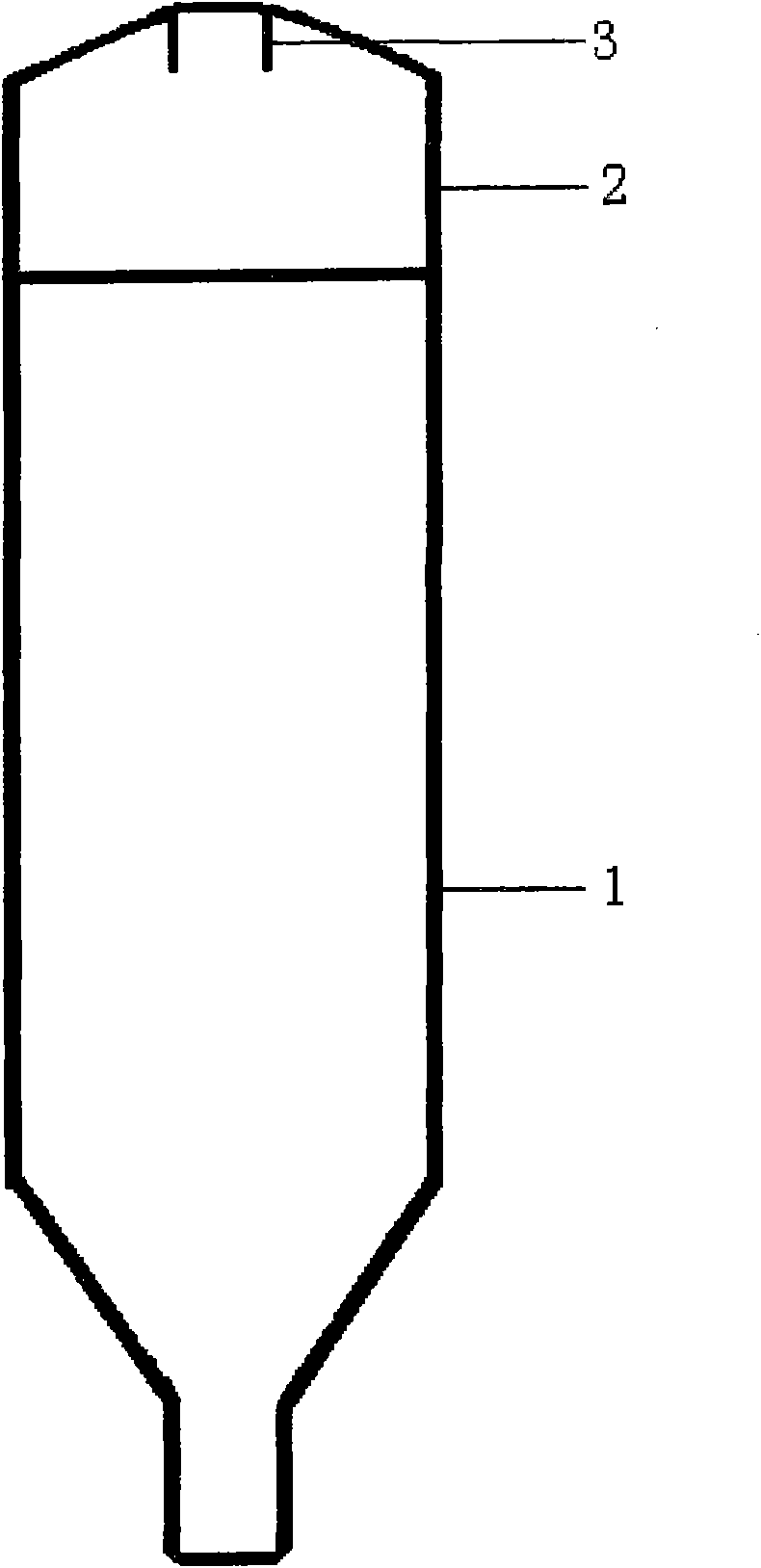
[0029] In order to achieve the above object, the present invention provides a new quartz tube structure, please refer to figure 1 As shown, it includes: a quartz body 1 and a quartz cap 2 covered therewith, wherein a quartz groove 3 is fixed on the inner top of the quartz cap 2; it is characterized in that:

[0030] The height of the cover quartz groove 3 is less than the depth of the quartz cap 2; this can avoid the oxidation of graphite in the welded quartz tube stone; the position of graphite in the quartz tube can be quantified by the depth of the quartz groove 3, and it can be realized by adding a verified temperature field heating temperature.

[0...


PUM


Abstract

The invention relates to a method for doping carbon in the gallium arsenide by using a silica tube for growing semi-insulated gallium arsenide. The method comprises the following steps: step 1: polycrystally synthesizing 7N Ga and 7N As to form a GaAs polycrystal; step 2: putting the synthesized GaAs polycrystal, seed crystal and B2O3 in a PBN crucible; step 3: putting the PBN crucible in a quartz body of the silica tube; step 4: fixing pure graphite in a silica groove on a silica cap of the silica tube; step 5: covering the quartz body and the silica cap, vacuumizing and welding the quartz body and the silica cap of the silica tube on oxyhydrogen flame; step 6: putting the welded silica tube in a VGF single crystal furnace for atmosphere doping and single crystal growth; and step 7: soaking the PBN crucible in methanol after the single crystal growth to obtain a GaAs single crystal and finish the preparation of the GaAs single crystal.

Description

technical field [0001] The invention relates to the VGF (vertical gradient solidification) technology of high-performance compound semiconductor SI-GaAs single crystal. The material is widely used mainly in the field of high-speed microelectronics, such as power amplifiers in radio frequency circuits, microwave monolithic integrated circuits (MMICs), etc. Background technique [0002] GaAs has excellent electrical properties such as high electron mobility, direct band gap, and wide band gap, and has been widely used in the fields of optoelectronics and microelectronics. For microelectronic ultra-high-speed circuits, semi-insulating SI-GaAs single crystals are required, that is, they have high resistance (greater than 10 7 Ω·cm). Generally speaking, high-purity GaAs itself is semi-insulating, but due to the complicated preparation process and high cost, industrial production uses compensation principles to achieve high resistance. [0003] With the continuous development o...

Claims


Application Information

Patent Timeline
IPC IPC(8): C30B29/42C30B11/00C30B31/06
Inventor 占荣惠峰赵有文
Owner INST OF SEMICONDUCTORS - CHINESE ACAD OF SCI
Why Eureka
Try Eureka