Stereo graphic pattern structure of circuit board and technique thereof

A patterning, circuit board technology, applied in printed circuits, printed circuit manufacturing, printed circuit components, etc., to achieve the effect of improving reliability, improving electroplating quality, and improving heat dissipation capacity

Active Publication Date: 2010-01-13
UNIMICRON TECH CORP
View PDF2 Cites 4 Cited by
  • Summary
  • Abstract
  • Description
  • Claims
  • Application Information

AI Technical Summary

Problems solved by technology

[0007] The invention provides a three-dimensional patterned structure of a circuit board and its process to solve the bottleneck of the aspect ratio of processes such as laser ablation and electroplating, thereby improving the reliability of the circuit board

Method used


Image

  • Stereo graphic pattern structure of circuit board and technique thereof
  • Stereo graphic pattern structure of circuit board and technique thereof
  • Stereo graphic pattern structure of circuit board and technique thereof

Examples


Embodiment Construction

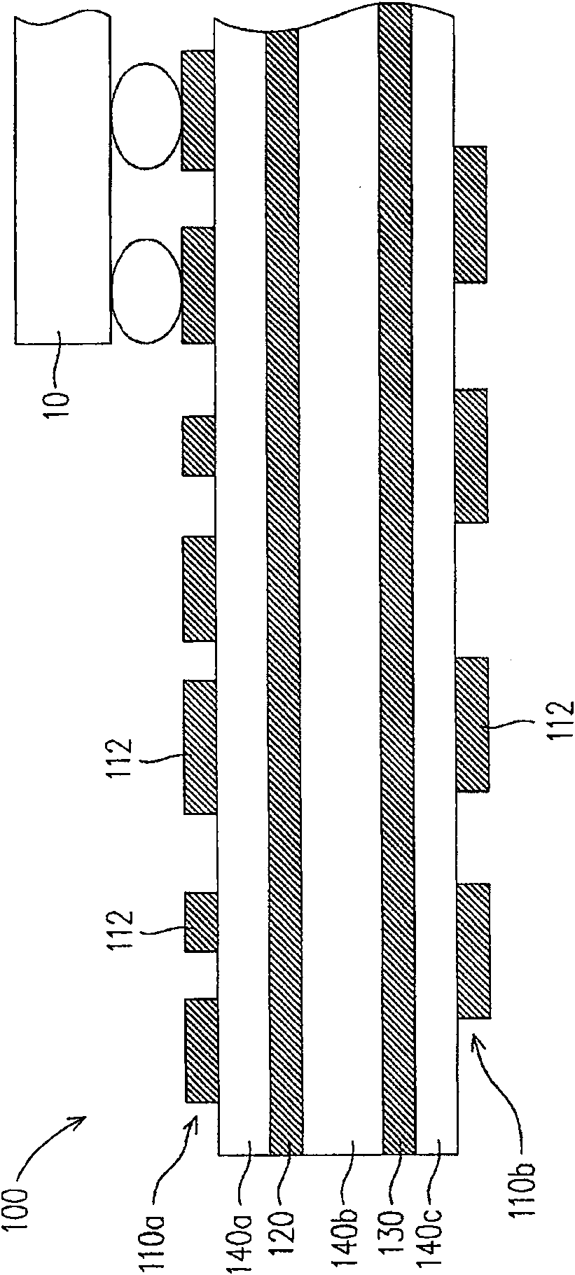
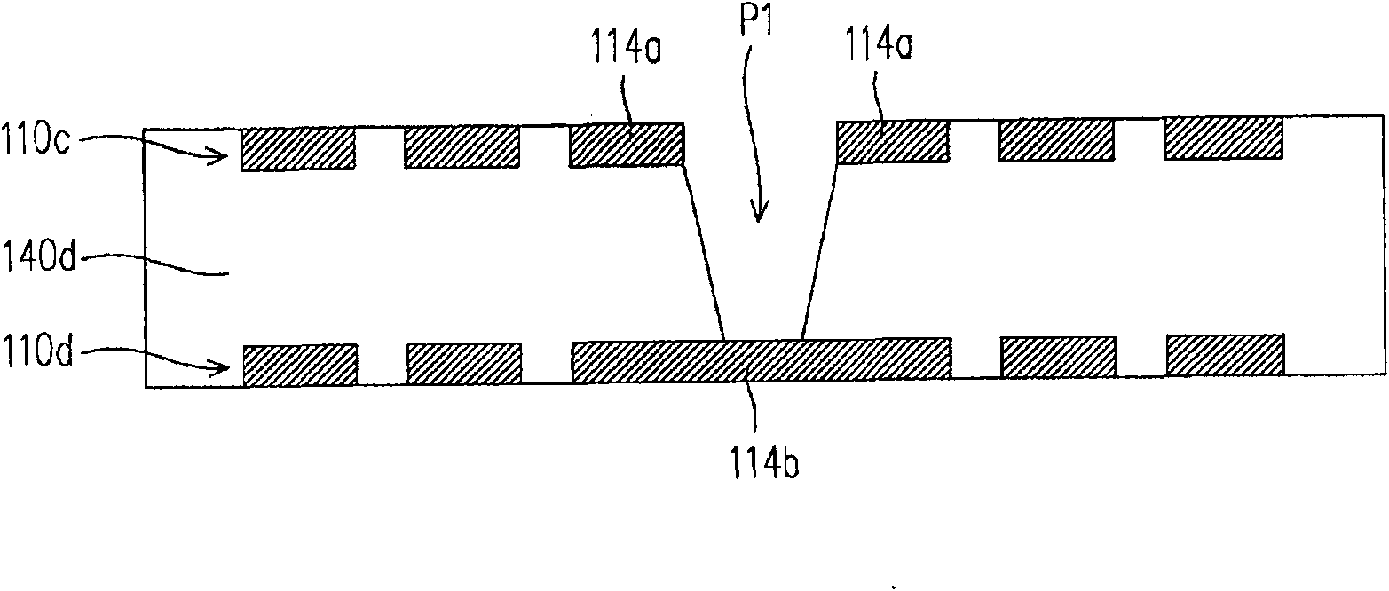
[0042] Figure 2A is a schematic cross-sectional view of a three-dimensional patterned structure of a circuit board according to an embodiment of the present invention, and Figure 2B is a schematic cross-sectional view of a three-dimensional patterned structure of a circuit board according to another embodiment of the present invention. It should be explained in advance that the circuit board can be a two-layer, four-layer, six-layer, eight-layer or more multi-layer circuit board, and the diagram is only represented by the configuration of the three-dimensional patterned structure. Figure 2A Can be used as the outermost circuit layer of the circuit board, while Figure 2BIt can be used as the circuit structure of any layer in the circuit board. Therefore, the circuit board can choose to complete the three-dimensional patterned structure of the present invention as the outermost circuit layer by layer-building method or lamination method after completing the inner layer cir...


PUM


Abstract

The invention discloses a tree-dimensional pattern structure of a circuit board and a circuit technology thereof. The three-dimensional pattern structure of the circuit board comprises a dielectric layer, at least one first three-dimensional pattern and at least one second three-dimensional pattern. The first three-dimensional pattern and the second three-dimensional pattern are configured at a same surface of the dielectric layer. The thickness of the first three-dimensional pattern is larger than the thickness of the second three-dimensional pattern. Due to that the heat-dissipation capacity of the first three-dimensional pattern increases with the increase of the thickness, the first three-dimensional pattern with relatively good heat-dissipation capacity can be used for enhancing the whole heat-dissipation capacity of the circuit board.

Description

technical field [0001] The present invention relates to a three-dimensional patterned structure of a circuit board and a trace process thereof, and in particular to a three-dimensional patterned structure with a plurality of different thicknesses in the same metal layer and its process. Background technique [0002] With the advancement of technology, electronic products such as cellular phones, notebook PCs, and personal digital assistants (PDAs) have become popular in modern society. Among the necessary parts of these electronic products, in addition to electronic components such as chips and passive components, the circuit boards carrying and configuring these chips and passive components are also indispensable and important. Component. [0003] Figure 1A It is a schematic cross-sectional view of a known circuit board. see Figure 1A , Figure 1A The circuit board 100 shown is a four-layer wiring board (four-layer wiring board), which is basically composed of two signa...

Claims


Application Information

Patent Timeline
Patent Type & Authority Patents(China)
IPC IPC(8): H05K1/00H05K3/00H05K1/09
Inventor 余丞博张启民
Owner UNIMICRON TECH CORP
Why Eureka
Try Eureka