Large-size glass substrate for photomask and making method, computer-readable recording medium, and mother glass exposure method
A technology for large glass substrates and photomasks, which is applied to the original components for photomechanical processing, photomechanical equipment, chemical instruments and methods, etc., and can solve the problems of increased weight of large glass substrates
- Summary
- Abstract
- Description
- Claims
- Application Information
AI Technical Summary
Problems solved by technology
Method used
Image
Examples
Embodiment 1
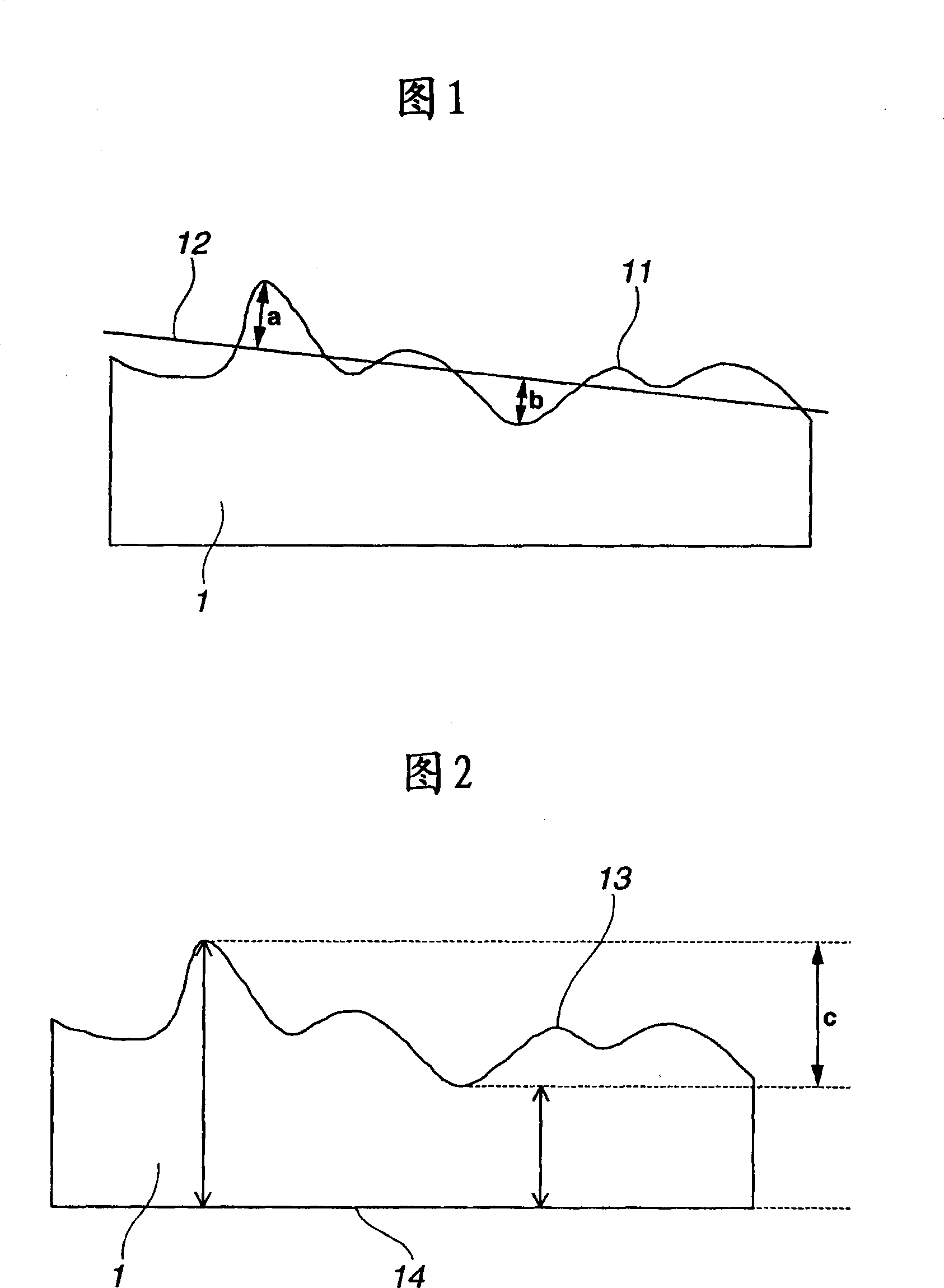
[0123] Use abrasive GC#600 (Fujimi Abrasive Co., Ltd.) and use a planetary motion double-sided grinder to grind to a size of 330mm×450mm (diagonal length is about 558mm) and a thickness of 5.3mm Synthetic quartz glass substrate material to prepare initial substrate or substrate material. The substrate material has a frontal flatness of 22 μm measured in a vertical posture (surface flatness / diagonal length=39×10 -6 ), a back flatness of 25 μm, and a parallelism of 3 μm, and the shape has a central portion higher than the least square plane.
[0124] Then, using the material strength and the support position of the substrate when held vertically, the deflection due to its own weight when held horizontally by the substrate material having a thickness of 5 mm after grinding was calculated. The deformation of the substrate and the stage are checked in advance from the amount of deformation of the virtual glass substrate material actually supported at an appropriate position in the...
Embodiment 2
[0134] The process of Example 1 was repeated except that a substrate material having a size of 520 mm×800 mm (diagonal length about 954 mm) and a thickness of 10.4 mm was used.
[0135] The proximity gap is measured substantially over the entire area using a laser displacement meter. The measured value near the gap includes a maximum value of 58 μm and a minimum value of 47 μm over the entire area except the peripheral region extending 4 cm from each side, and the gap error is 11 μm.
Embodiment 3
[0137] The process of Example 1 was repeated except that a substrate material having a size of 850 mm×1200 mm (diagonal length about 1471 mm) and a thickness of 10.4 mm was used.
[0138] The proximity gap is measured substantially over the entire area using a laser displacement meter. The measured value near the gap includes a maximum value of 59 μm and a minimum value of 47 μm over the entire area except the peripheral region extending 4 cm from each side, and the gap error is 12 μm.
PUM
| Property | Measurement | Unit |
|---|---|---|
| thickness | aaaaa | aaaaa |
| length | aaaaa | aaaaa |
| length | aaaaa | aaaaa |
Abstract
Description
Claims
Application Information

