Supercharge Your Innovation With Domain-Expert AI Agents!

Method of monitoring depositing temperature of cu seed layer and method for forming cu layer by using the same

A copper seed layer, deposition temperature technology, applied in thermometers, thermometers with physical/chemical changes, coatings, etc., can solve problems such as trouble and difficulty

Inactive Publication Date: 2007-08-01
DONGBU ELECTRONICS CO LTD
View PDF0 Cites 0 Cited by
  • Summary
  • Abstract
  • Description
  • Claims
  • Application Information

AI Technical Summary

Problems solved by technology

[0007] However, instead of directly confirming whether condensation has occurred in the Cu seed layer deposited on the substrate, this temperature determination process can be a very cumbersome and difficult task.

Method used


Image

  • Method of monitoring depositing temperature of cu seed layer and method for forming cu layer by using the same

Examples


Embodiment Construction

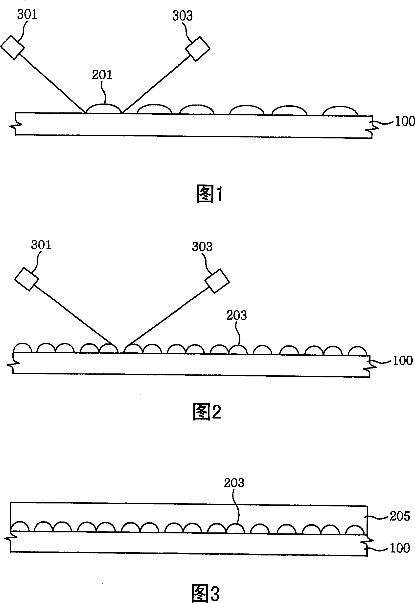
[0029] Embodiments of the present invention relate to a method capable of monitoring the deposition temperature of a Cu seed layer based on the light reflectance of the Cu seed layer. The embodiment of the present invention also relates to a method for forming a Cu layer.

[0030] According to an embodiment, after depositing the Cu seed layer, the light reflectance of the Cu seed layer is measured, so that it can be determined based on the measured light reflectance whether condensation has occurred in the Cu seed layer, thereby providing a Method for monitoring deposition temperature of Cu seed layer. This method of monitoring the deposition temperature of the Cu seed layer also prevents the subsequently electroplated Cu layer from being damaged due to the agglomeration phenomenon of the Cu seed layer.

[0031] Referring to FIGS. 1 and 2, a substrate 100 is installed in a Cu seed layer deposition apparatus (not shown). The first Cu seed layer 201 or the second Cu seed layer...


PUM

PropertyMeasurementUnit
reflectanceaaaaaaaaaa

Abstract

A method for monitoring a deposition temperature of a Cu seed layer by measuring an optical reflectivity of the Cu seed layer deposited on a substrate; and estimating the deposition temperature of the Cu seed layer by comparing the measured optical reflectivity with a reference optical reflectivity of a reference Cu seed layer in which an agglomeration phenomenon has not happened. The estimating step includes computing the deposition temperature of the Cu seed layer at a temperature higher than about -25 DEG C. which is a reference deposition temperature for depositing the reference Cu seed layer if the measured reflectivity is smaller than the reference optical reflectivity.

Description

technical field [0001] The present invention relates to a method for monitoring the deposition temperature of a copper seed layer and a method for forming a copper layer, more specifically, to a method capable of directly monitoring the deposition temperature of a copper seed layer based on whether condensation has occurred, and a A method of forming a copper layer more uniformly by using this monitoring method. Background technique [0002] As semiconductor devices tend to be more integrated and operate at higher speeds, methods of forming metal wirings using a copper (Cu) layer have been proposed. In particular, logic devices using a design rule of 130nm or less have implemented interconnection wiring with a Cu damascene process. [0003] The forming process of the Cu layer for the wiring structure includes the following steps: firstly, a Cu seed layer is formed; then, a thicker Cu layer is electroplated on the Cu seed layer. A damascene process has been introduced for C...

Claims


Application Information

Patent Timeline
Patent Type & Authority Applications(China)
IPC IPC(8): G01N21/55C25D5/34C25D5/54C25D7/12H05K3/00H01L21/288H01L21/445
CPCH05K1/0269H05K3/181G01K11/125C23C14/547C23C14/185C23C14/541H01L21/28H01L22/00
Inventor 朱星中李汉春
Owner DONGBU ELECTRONICS CO LTD
Features
  • R&D
  • Intellectual Property
  • Life Sciences
  • Materials
  • Tech Scout
  • Unparalleled Data Quality
  • Higher Quality Content
  • 60% Fewer Hallucinations
Learn More