Method for manufacturing an electric device with a layer of conductive material contacted by nanowire
A technology of conductive material layers and electronic devices, applied in the direction of electric solid devices, semiconductor devices, electrical components, etc.
- Summary
- Abstract
- Description
- Claims
- Application Information
AI Technical Summary
Problems solved by technology
Method used
Image
Examples
Embodiment Construction
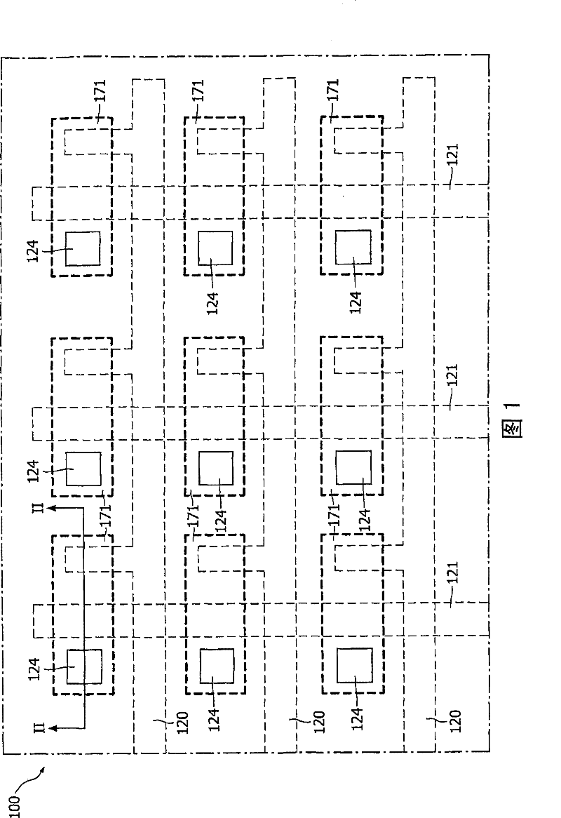
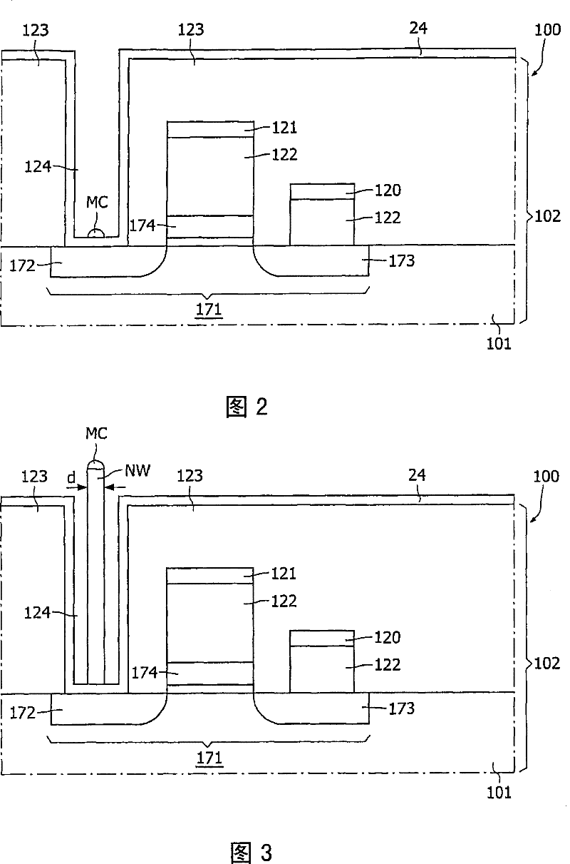
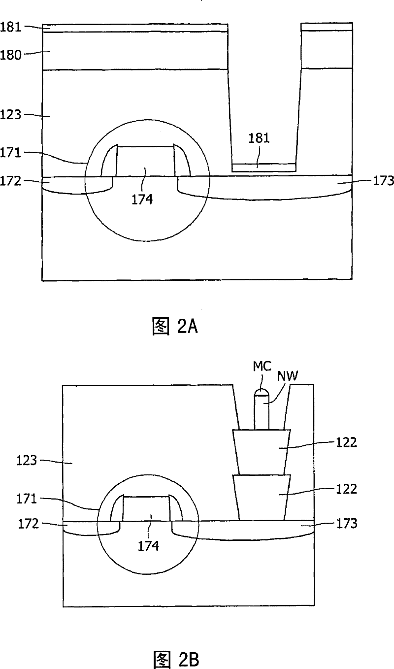
[0065] Figure 1~5 Various stages of fabrication are shown for an embodiment of an electronic device 100 having a base body 102 comprising a substrate 101 which may comprise, for example, a monocrystalline p-doped silicon semiconductor wafer. The base also includes an array of selection devices 171 . exist Figure 1~5 In the illustrated embodiment, electronic device 100 has a 3x3 array, but the invention is not limited to arrays of this size, nor to arrays of this shape. The base body 102 also includes a grid of select lines 120 , 121 , so that each memory cell is individually accessible via a respective select line 120 , 121 connected to a respective select device 171 .
[0066] exist Figure 1~5 In the illustrated embodiment, the selection device 171 comprises a Metal Oxide Semiconductor Field Effect Transistor (MOSFET), and more specifically, an NMOS transistor. The MOSFET has an n-doped source region 172 , an n-doped drain region 173 and a gate region 174 . Source reg...
PUM
| Property | Measurement | Unit |
|---|---|---|
| thickness | aaaaa | aaaaa |
| thickness | aaaaa | aaaaa |
| diameter | aaaaa | aaaaa |
Abstract
Description
Claims
Application Information


