Program bootstrap method after chip power-on

A program and chip technology, applied in the field of chip design, can solve the problems that the program packaging method is only applicable, uncertain, and difficult to meet the requirements of complex and changeable embedded systems, and achieves the effect of facilitating firmware debugging and increasing security.

Active Publication Date: 2007-08-22
HANGZHOU SYNOCHIP DATA SECURITY TECH CO LTD
View PDF1 Cites 42 Cited by
  • Summary
  • Abstract
  • Description
  • Claims
  • Application Information

AI Technical Summary

Problems solved by technology

[0004] 1. The program encapsulation method is only applicable to NAND FLASH;
[0005] 2. There is no method for configuring the chip during the boot process; when the chip is powered on, some internal registers or interfaces are in the default state, and some are in an uncertain state, so initialization is required first, and it needs to be based on different application requirements configure
Therefore, this invention applies for the selection of the task number, because of the real-time nature of the embedded software operation, whether it is manually or automatically selecting the task number to load the program, it is difficult to meet the complex and changeable embedded system requirements;

Method used


Image

  • Program bootstrap method after chip power-on
  • Program bootstrap method after chip power-on

Examples


Embodiment Construction

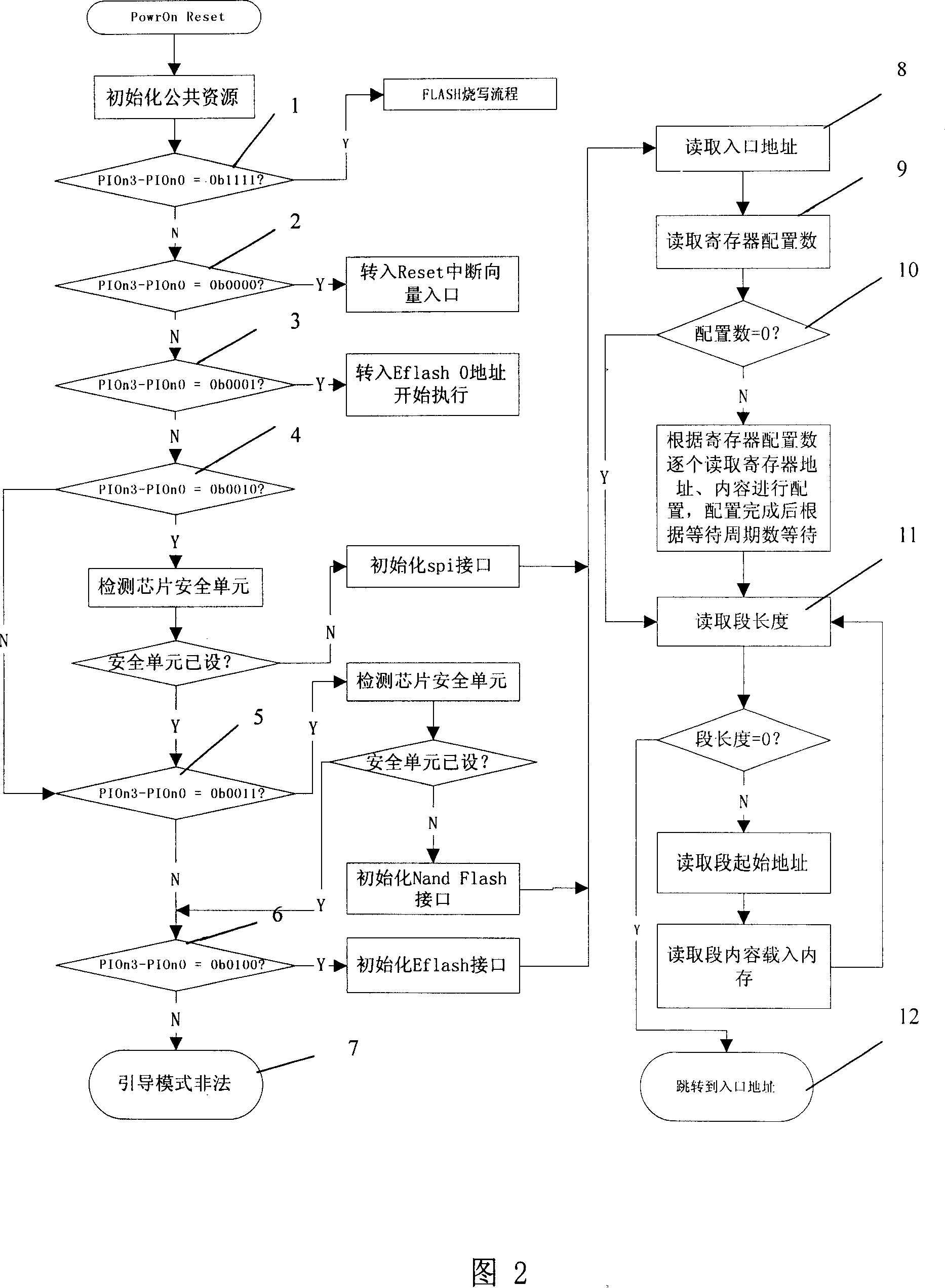
[0049] The present invention will be further described below in conjunction with the accompanying drawings, and the accompanying drawings and examples are only used for explanation and description, and are not intended to limit the scope of the present invention.

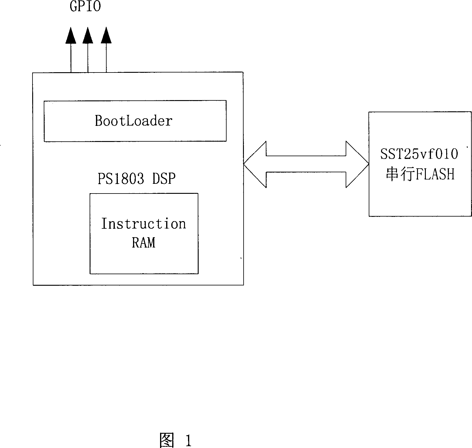
[0050] Table 1 represents a schematic diagram of the method program packaging of the present invention, and the application program packaged with this packaging method can be stored in NOR FLASH, EPROM or NAND FLASH on-chip, or can be stored in NOR FLASH, EPROM or NAND FLASH outside the chip, and serial row in EEPROM or FLASH;

[0051] The application data packet encapsulated by this encapsulation method is divided into three parts, that is, the first part is the entry address field, the second part is the register configuration field, and the third part is the program segment field.

[0052] The entry address field stores the execution first address after the program is loaded;

[0053] The register configuration ...


PUM


Abstract

The invention relates to a guiding procedure for a chip after loading electricity. Its characteristics are as following: the procedure is stored in a nonvolatile storage, and the procedure is packaged, and the packaged data-application includes: an import-address domain, a configuration register domain and a procedure domain, of which: the import-address domain is used for storing the first address of implementation after loading the procedure, and the configuration register domain is used for storing the number of configured registers and the addresses of registers, configuration content and the clock cycle for configuration in the process, and the procedure domain is used for storing procedures. The guiding procedure includes: it reads data packets according to packaging format, and it checks the addresses of procedures and length of information stored in the non-volatile memory, and it loads the procedures to the operation memory for implementing procedures.

Description

technical field [0001] The invention belongs to the technical field of chip design, and in particular relates to a method allowing selection of a boot program from on-chip FLASH / EEPROM or ROM or from off-chip serial FLASH / EEPROM or NAND FLASH. Background technique [0002] The development of processors basically follows Moore's Law, the main frequency and complexity are doubling every year, and the resources inside the chip are becoming more and more abundant. However, FLASH and ROM are the most commonly used program storage bodies. In addition to the increase in capacity, there has been no fundamental breakthrough in other technical performances for several years. The traditional method of storing application programs in off-chip Nor Flash (or non-type flash memory) or ROM (read-only memory) and directly executing them has become a bottleneck for overall system performance improvement. So now the processors are embedded with a large amount of high-speed SRAM (Static Random...

Claims


Application Information

Patent Timeline
Patent Type & Authority Applications(China)
IPC IPC(8): G06F9/445
Inventor 邱柏云裴育
Owner HANGZHOU SYNOCHIP DATA SECURITY TECH CO LTD
Why Eureka
Try Eureka